Methods and apparatus for processing the surface of a microelectronic workpiece

Inactive Publication Date: 2001-10-30
SEMITOOL INC
View PDF37 Cites 94 Cited by
  • Summary
  • Abstract
  • Description
  • Claims
  • Application Information

AI Technical Summary

Benefits of technology

The reactor as may also include a backing member and a drive mechanism in an assembly in which the backing member and contact assembly are moved relative to one another by the drive mechanism between a workpiece loading state and a workpiece processing state. In the workpiece

Problems solved by technology

This non-uniform distribution of current across the wafer, in turn, causes non-uniform deposition of the plated metallic material.
But such thieving techniques add to the complexity of electroplating equipment, and increase maintenance requirements.
Another problem with electroplating of wafers concerns efforts to prevent the electric contacts themselves from being plated during the electroplating process.
While it is possible to provide sealing mechanisms for discrete electrical contacts, such arrangements typically cover a significant area of the wafer surface, and can add complexity to the electrical contact design.
Electroplated material may not adhere well to the exposed barrier layer material, and is therefore prone to peeling off in subsequent wafer processing steps.
Further, metal that is electroplated onto the barrier layer within the reactor may flake off during the electroplating process thereby adding particulate contaminants to the electroplating bath.
Such contaminants can adversely affect the overall electroplating process.
The specific metal to b

Method used


Image

  • Methods and apparatus for processing the surface of a microelectronic workpiece
  • Methods and apparatus for processing the surface of a microelectronic workpiece
  • Methods and apparatus for processing the surface of a microelectronic workpiece

Examples


Example

A first embodiment of 
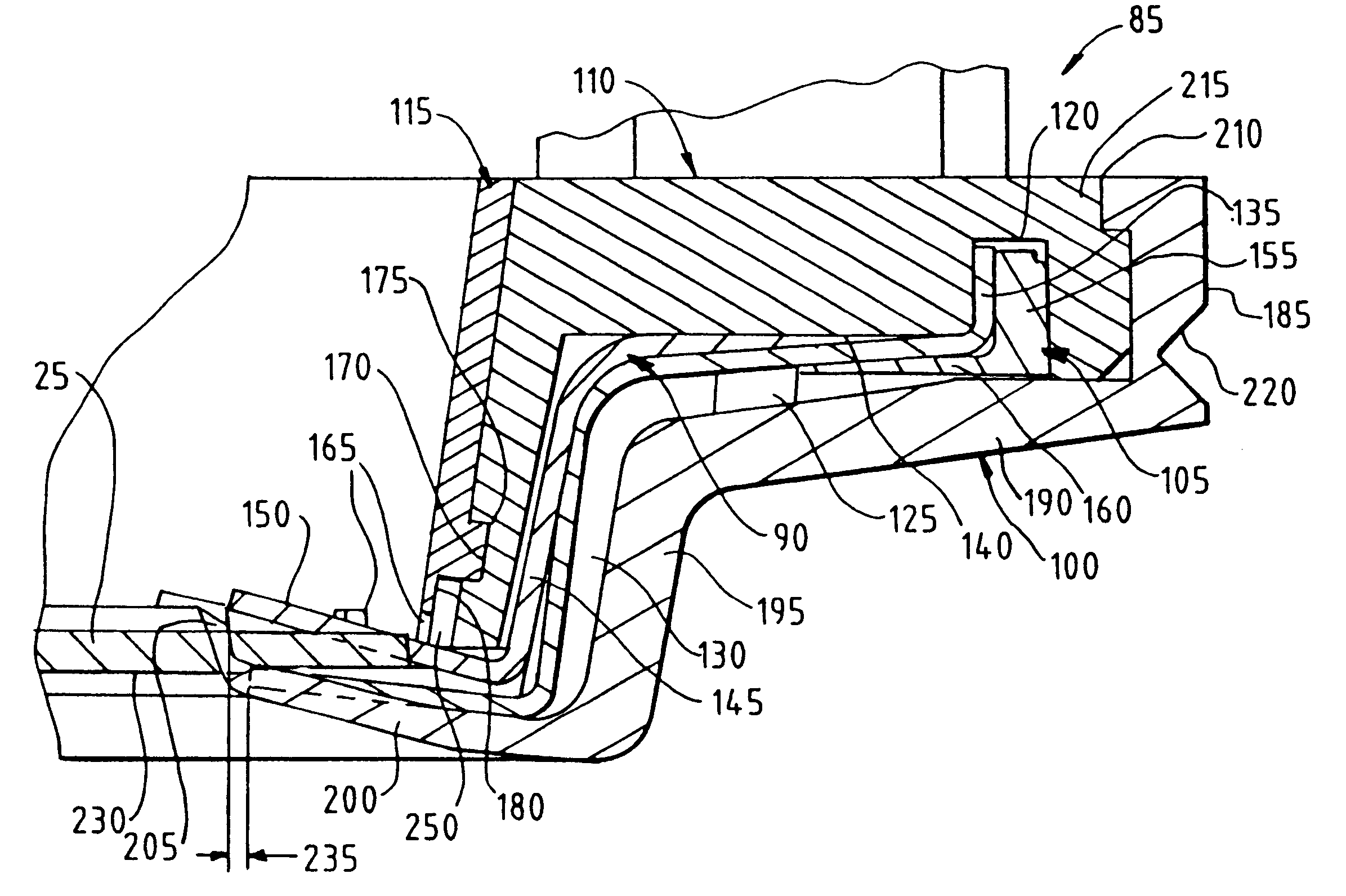
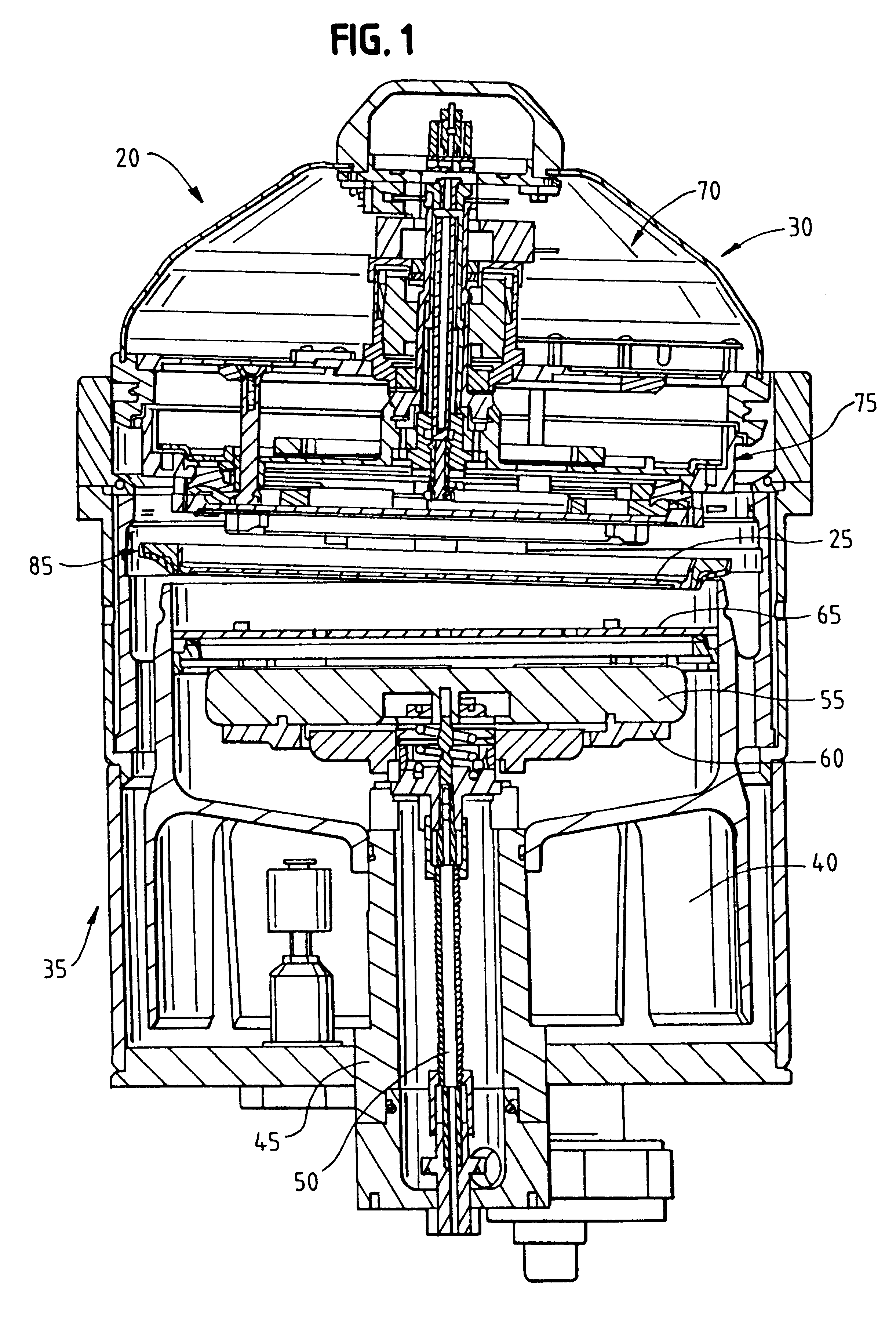
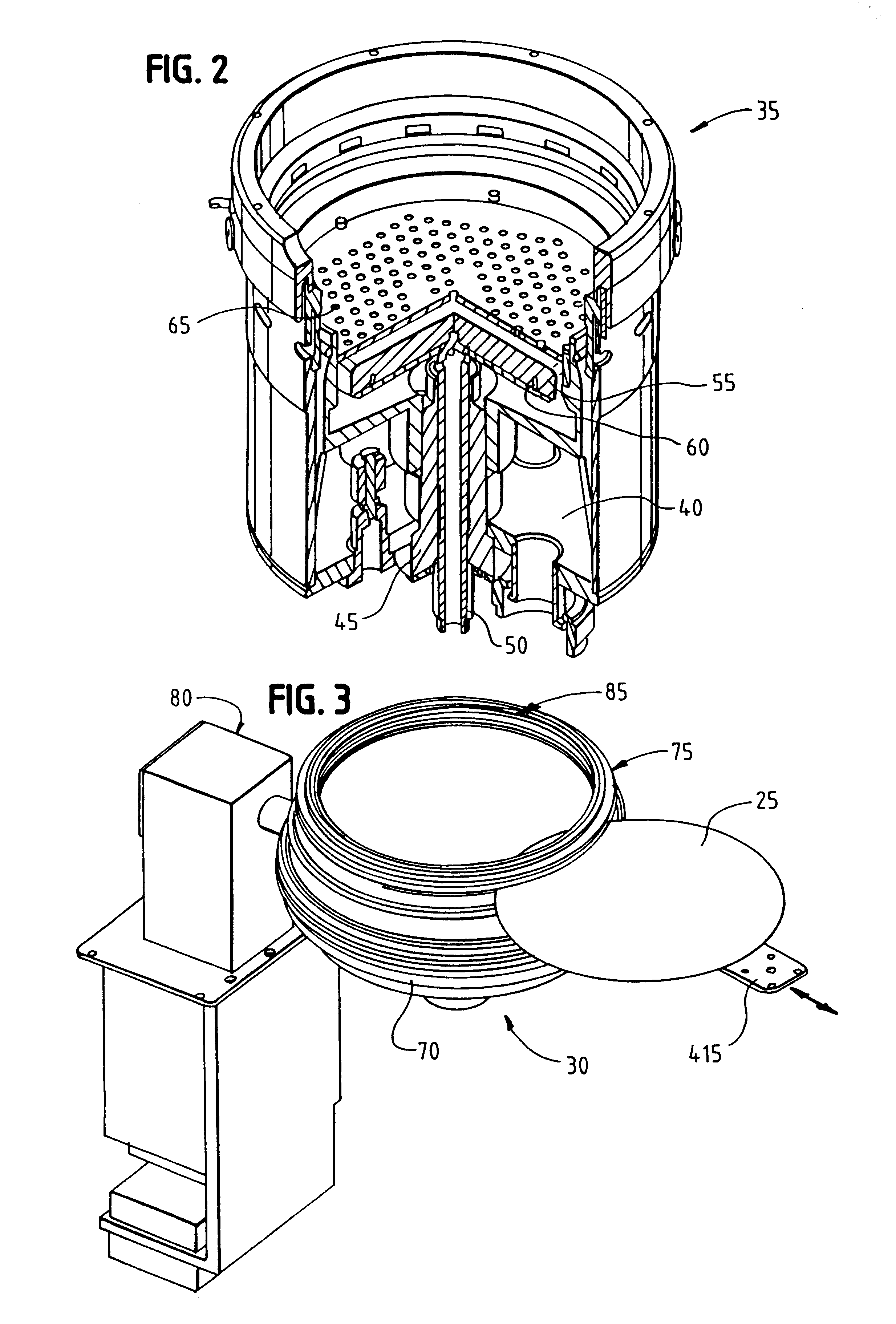
a Bellville ring contact assembly is illustrated generally at 600 in in FIGS. 18-20. As illustrated, the contact assembly 600 comprises a conductive contact mount member 605, a Bellville ring contact 610, a dielectric wafer guide ring 615, and an outer body member 625. The outer, common portion 630 of the Bellville ring contact 610 includes a first side that is engaged within a notch 675 of the conductive base ring 605. In many respects, the Belleville ring contact assembly of this embodiment is similar in construction with the flexure contact assembly 85 described above. For that reason, the functionality of many of the structures of the contact assembly 600 will be apparent and will not be repeated here.

Preferably, the wafer guide ring 615 is formed from a dielectric material while contact mount member 605 is formed from a single, integral piece of conductive material or from a dielectric or other material that is coated with a conductive material at its exte...


PUM

PropertyMeasurementUnit
Dielectric polarization enthalpyaaaaaaaaaa
Radiusaaaaaaaaaa
Electrical conductoraaaaaaaaaa

Abstract

A reactor for plating a metal onto a surface of a workpiece is set forth. The reactor comprises a reactor bowl including an electroplating solution disposed therein and an anode disposed in the reactor bowl in contact with the electroplating solution. A contact assembly is spaced from the anode within the reactor bowl. The contact assembly includes a plurality of contacts disposed to contact a peripheral edge of the surface of the workpiece to provide electroplating power to the surface of the workpiece. The contacts execute a wiping action against the surface of the workpiece as the workpiece is brought into engagement therewith The contact assembly also including a barrier disposed interior of the plurality of contacts. The barrier includes a member disposed to engage the surface of the workpiece to assist in isolating the plurality of contacts from the electroplating solution. In one embodiment, the plurality of contacts are in the form of discrete flexures while in another embodiment the plurality of contacts are in the form of a Belleville ring contact. A flow path may be provided in the contact assembly for providing a purging gas to the plurality of contacts and the peripheral edge of the workpiece. The purging gas may be used to assist in the formation of the barrier of the contact assembly. A combined electroplating/electroless plating tool and method are also set forth.

Description

Production of semiconductor integrated circuits and other microelectronic devices from workpieces such as semiconductor wafers typically requires formation of one or more metal layers on the wafer. These metal layers are used, for example, to electrically interconnect the various devices of the integrated circuit. Further, the structures formed from the metal layers may constitute microelectronic devices such as read / write heads, etc.The microelectronic manufacturing industry has applied a wide range of metals to form such structures. These metals include, for example, nickel, tungsten, solder, platinum, and copper. Further, a wide range of processing techniques have been used to deposit such metals. These techniques include, for example, chemical vapor deposition (CVD), physical vapor deposition (PVD), electroplating, and electroless plating. Of these techniques, electroplating and electroless plating tend to be the most economical and, as such, the most desirable. Electroplating a...

Claims


Application Information

Patent Timeline
IPC IPC(8): C25D7/12
CPCC25D17/001C25D7/123
Inventor WOODRUFF, DANIEL J.HANSON, KYLE M.OBERLITNER, THOMAS H.CHEN, LINLINPEDERSEN, JOHN M.ZILA, VLADIMIR
Owner SEMITOOL INC
Why Eureka
Try Eureka