Data processor with built-in DRAM

a data processor and built-in dram technology, applied in the direction of detecting faulty computer hardware, error detection/correction, instruments, etc., can solve the problem of unnecessary wiring rounding, difficult to obtain the optimum chip size, and the inability to use a macro cell of the existing graphic controller, etc. problem, to achieve the effect of increasing the memory address depth

Inactive Publication Date: 2001-12-04
RENESAS ELECTRONICS CORP
View PDF17 Cites 26 Cited by
  • Summary
  • Abstract
  • Description
  • Claims
  • Application Information

AI Technical Summary

Benefits of technology

A further object of the present invention is to realize an incorporated image memory having an

Problems solved by technology

Also, unnecessary drawing-around of wiring is caused in order to provide an interface with the graphic controller.
Namely, in the case where the conventional general purpose standard DRAM or synchronous DRAM is incorporated as it is, it is difficult to obtain the optimum chip size.
Also, since the graphic controller is filled in a vacant space of the DRAM, it becomes impossible

Method used


Image

  • Data processor with built-in DRAM
  • Data processor with built-in DRAM
  • Data processor with built-in DRAM

Examples


Embodiment Construction

.

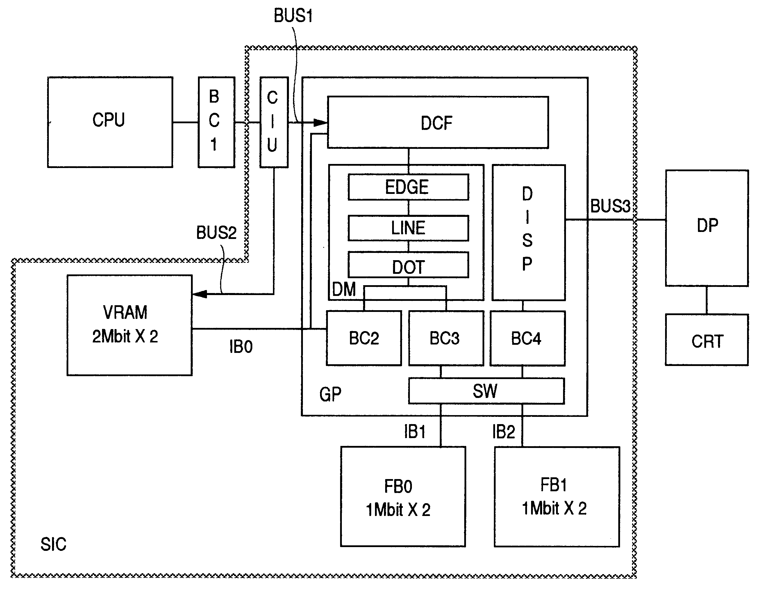
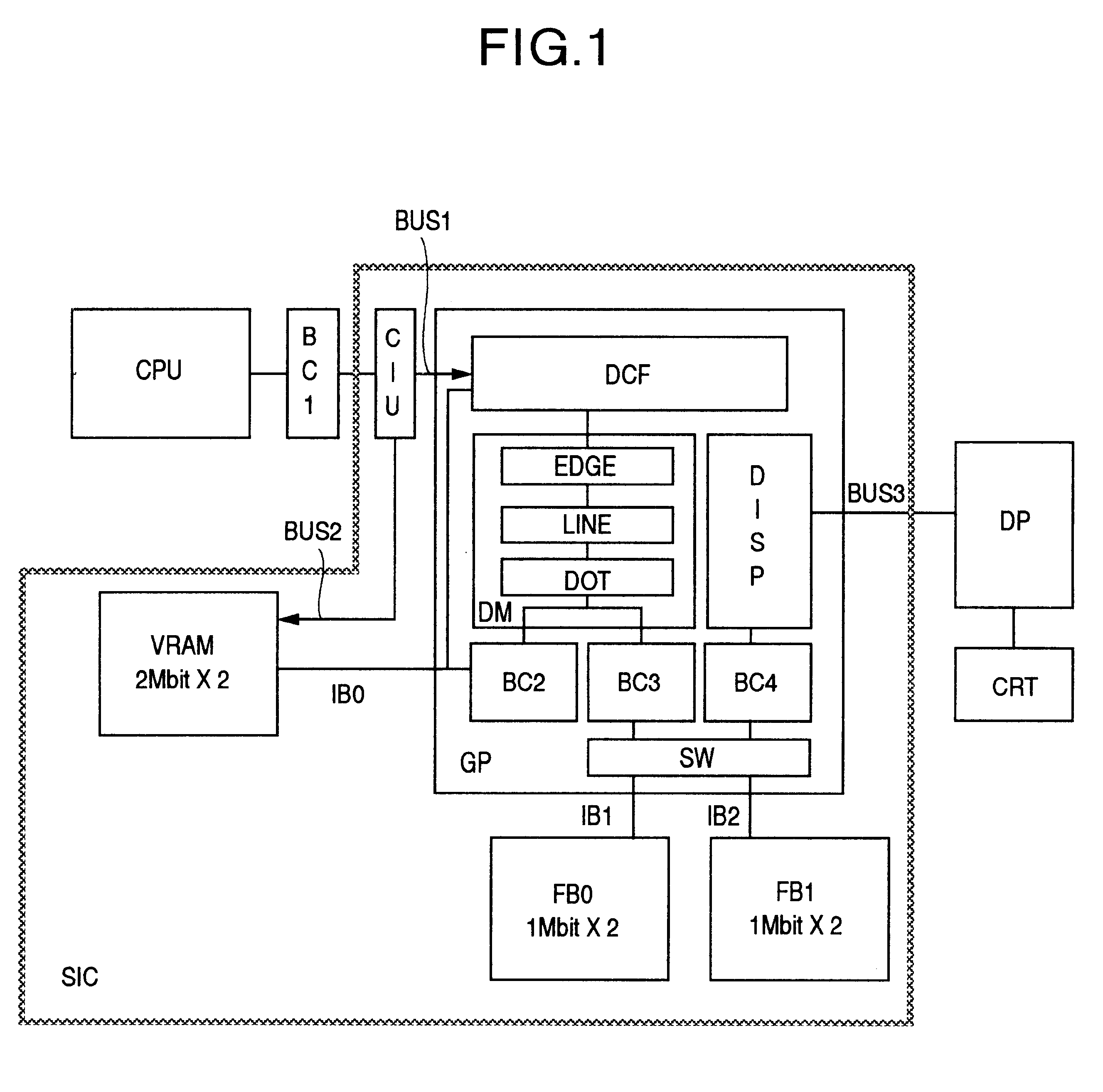
FIG. 1 shows an example of a system which uses a semiconductor integrated circuit device according to an embodiment the present invention. The system shown in FIG. 1 forms a part of a data processing system such as a personal computer or an amusement equipment.

A semiconductor integrated circuit device SIC is composed of an image processor GP, a command / source data image memory (hereinafter referred to as command memory) VRAM and drawing / display memories (hereinafter referred to as drawing memories) FB0 and FB1. The semiconductor integrated circuit device SIC is formed on one semiconductor substrate such as a silicon substrate and is resin-sealed (or sealed in a plastic package). The semiconductor integrated circuit device SIC is connected to a central processing unit CPU and a CRT control circuit DP.

The central processing unit CPU makes an access to the image processor GP through a bus control circuit BC1. In the image processor GP, an output from the bus control circuit BC1 divide...


PUM


Abstract

The present invention may be introduced to an architecture such as a personal computer or an amusement equipment for realizing a high-speed graphic processing. When a frame buffer, a command memory and an image processor are incorporated in one chip in order to improve the drawing performance of an image processing device, a test terminal and a test bus are provided in the image processing device, and a test port is provided in each memory module and is connected to a common test bus, so that a content of each incorporated memory module is monitored externally when it is tested. Thereby, it is possible to employ the conventional testing method itself in testing the memory modules.

Description

The present invention relates to a semiconductor integrated circuit device, and more particularly to a semiconductor integrated circuit device in which a data processing device for performing image processing and a memory device for storing image data or instructions are incorporated.In recent years, personal computers have pushed into the field of work stations with intent to realize alternate for large-size computers by the network configuration of work stations. Also, an architecture for realizing a low-cost and high-speed graphic processing has recently been needed with the advance of home amusement equipments. In particular, a modified sprite processing for freely mapping source data of rectangles forms the basis of a three-dimensional graphics processing and is expected to have a drawing performance on the order of several ten thousands of polygons per second in order to realize more real display.In order to improve the drawing performance of graphic LSI, a labor is taken for ...

Claims


Application Information

Patent Timeline
IPC IPC(8): G06T1/20G11C29/04G11C29/48G06F11/22G06F11/267
CPCG06F11/2284G06T1/20G11C29/48G06F11/2236G11C11/407
Inventor YAMAGISHI, KAZUSHIGESATO, JUNMIYAMOTO, TAKASHI
Owner RENESAS ELECTRONICS CORP
Why Eureka
Try Eureka