Apparatus and method for performing a defect leakage screen test for memory devices

a defect leakage and memory device technology, applied in semiconductor/solid-state device testing/measurement, instruments, transistors, etc., can solve problems such as potential reliability problems, cell weakness, and time-consuming process, and the ability to characterize retention related single bit failures remains

Inactive Publication Date: 2001-12-11
QIMONDA +1
View PDF24 Cites 35 Cited by
  • Summary
  • Abstract
  • Description
  • Claims
  • Application Information

AI Technical Summary

Problems solved by technology

These cells are considered weak and are potential reliability problems.
These weaker cells are usually the result of defects.
Although a weaker cell may function normally under typical operating conditions after initial fabrication, it may degrade with time or stress, and later fail after module assembly or after burn-in stress testing, or in a customer application.
The PFA, however, is a very thorough but time consuming process.
Thus, the ability to characterize retention related single bit failures remains a challenge in the art that has, to date, been performed by inefficiently varying the refresh cycle time of the device.
Weaker read output charge can be the result of several possible defects or abnormalities within the cell, such as high junction leakage current, high sub-threshold current, parasitic leakage paths, low cell capacitance, and high connection resistance.
It remains difficult under the prior art test methods to ascertain which defect caused the failure.

Method used


Image

  • Apparatus and method for performing a defect leakage screen test for memory devices
  • Apparatus and method for performing a defect leakage screen test for memory devices
  • Apparatus and method for performing a defect leakage screen test for memory devices

Examples


Embodiment Construction

)

In describing the preferred embodiment of the present invention, reference will be made herein to FIGS. 2-7 of the drawings in which like numerals refer to like features of the invention. Features of the invention are not necessarily shown to scale in the drawings.

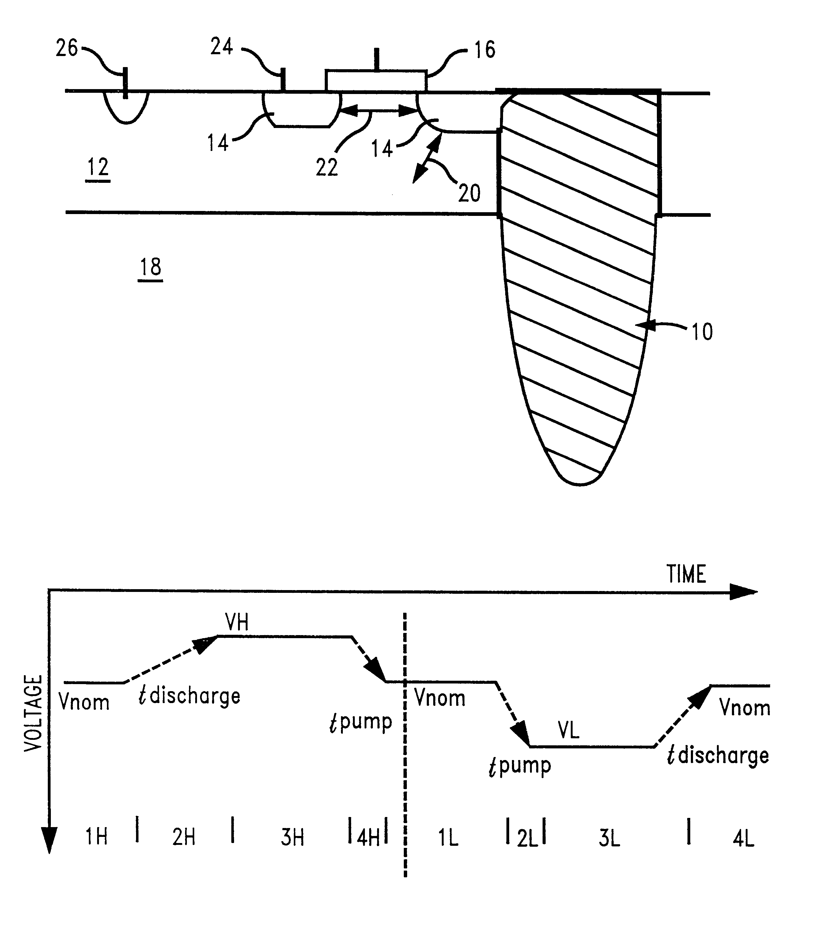
A Defect Leakage Screen Test apparatus is introduced to eliminate or reduce steps in the failure analysis process of memory devices, such as DRAM cells, or to eliminate the necessity of a Physical Failure Analysis (PFA) in its entirety. The introduced test procedure is aimed to characterize special single bit failures due to leakage current, junction leakage current, or sub-threshold leakage current. Importantly, this test method can be applied at the package level. The test method employs a test mode initial program load (IPL) variation of the cell transfer device back-bias voltage or p-well voltage (v.sub.bb). The ability to vary v.sub.bb makes it possible to identify which type of leakage is likely causing a cell to be...


PUM


Abstract

A Defect Leakage Screen Test apparatus and method is introduced to eliminate or reduce steps in the failure analysis process of memory devices, such as DRAM cells, or to eliminate the necessity for the application of a physical failure analysis on the memory device.Special single bit failures due to leakage current, junction current, or threshold leakage current, are characterized by varying the p-well voltage of the memory device during the read operation of the test.The p-well voltage is varied with a test code Initial Program Load (IPL). Additional logic is provided on the memory IC to decode the IPL logic signals.In order to perform the p-well varying test, the memory device is provided with the following: IPL decoding logic; a reference voltage generator; an IPL voltage reference multiplexor; a p-well voltage feed-back circuit; and a differential amplifier circuit.

Description

1. Field of the InventionThe present invention relates to semiconductor devices and more specifically to dynamic memory devices, such as dynamic random access memory devices (DRAMs).2. Description of Related ArtAt the end of the testflow for every DRAM is the Burn-In module stress test and the Final module test. The purpose of these tests is to screen out all stress induced cell failures due to packaging and Burn-In. These tests perform a critical screening and characterization for memory cells, such as DRAM cells, which aid in identifying the retention time related failures at the module level. Retention time is determined by leakage current which has the effect of discharging the cell's high voltage or "1's" level to a lower voltage that makes it fail the read "1" operation. Leakage current occurs normally in DRAM cells, as predicted by semiconductor physics, but at sufficiently low values that correspond to retention times of several seconds. Present day DRAMs are tested and guar...

Claims


Application Information

Patent Timeline
Patent Type & Authority Patents(United States)
IPC IPC(8): G11C29/50G11C29/04G11C29/02G01R31/28G01R31/3183G11C11/401H01L21/66H01L21/8242H01L27/108
CPCG11C29/02G11C29/025G11C29/028G11C29/50G11C11/401G11C2029/5004G11C2029/5006
Inventor CLINTON, MICHAEL P.ENK, KLAUS G. F.HOUGHTON, RUSSELL J.NORRIS, ALAN D.SCHNELL, JOSEF T.
Owner QIMONDA
Why Eureka
Try Eureka