Vector register addressing

a vector register and register technology, applied in the field of data processing, can solve the problems of disadvantageously large overhead in cost and complexity, difficult to make global changes to the vector length without having to resort to self-modifying code, and disadvantageously inefficien

Inactive Publication Date: 2001-12-18
ARM LTD
View PDF12 Cites 115 Cited by
  • Summary
  • Abstract
  • Description
  • Claims
  • Application Information

AI Technical Summary

Benefits of technology

The invention allows the use of simple to implement contiguous block memory access instructions without the cost and complexity of a scatter gather mechanism. The increment (variable between vectors) that is applied to the register address upon each iteration permits the system to step through non-adjacent data value thereby selecting the appropriate matrix, real or imaginary value to be processed. In practice it has been found that the restriction to a fixed increment between register addresses within execution of a vector instruction is not a significant constraint since many important real-life tasks match this behaviour. In summary, the system is able to exploit efficient block memory access instructions to a memory in which the data is arranged in a flat form whilst preserving the vector processing ability to specify a sequence of operations with a single instruction.
This feature effectively allows additional instructions to be encoded by virtue of the register number used rather than scarce opcode bits.

Problems solved by technology

Whilst the Cray 1 architecture provides a great deal of flexibility in the operations that can be supported is requires a disadvantageously large overhead in term of cost and complexity.
The provision of the vector length within the instruction itself makes it difficult to make global changes to the vector length without having to resort to self-modifying code.
This is disadvantageously inefficient.

Method used


Image

  • Vector register addressing
  • Vector register addressing
  • Vector register addressing

Examples


Embodiment Construction

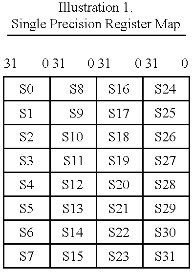
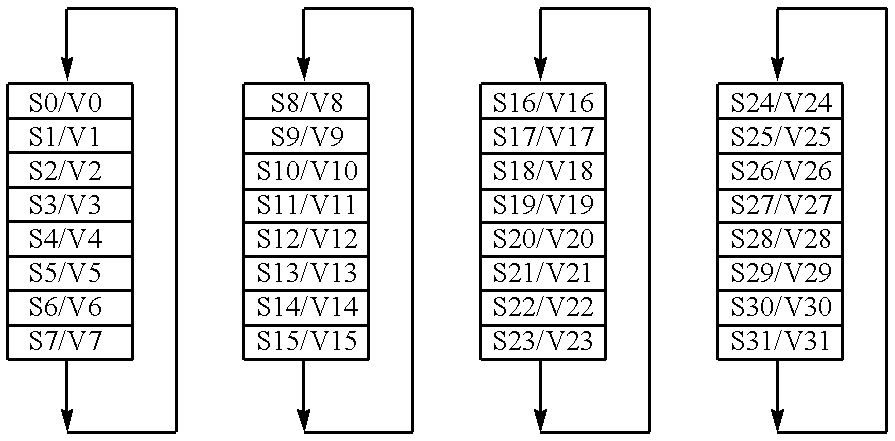
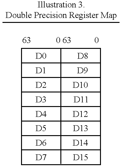
FIG. 1 illustrates a data processing system 22 comprising a main processor 24, a floating point unit coprocessor 26, a cache memory 28, a main memory 30 and an input / output system 32. The main processor 24, the cache memory 28, the main memory 30 and the input / output system 32 are linked via a main bus 34. A coprocessor us 36 links the main processor 24 to the floating point unit coprocessor 26.

In operation, the main processor 24 (also referred to as the ARM core) executes a stream of data processing instructions that control data processing operations of a general type including interactions with the cache memory 28, the main memory 30 and the input / output system 32. Embedded within the stream of data processing instructions are coprocessor instructions. The main processor 24 recognises these coprocessor instructions as being of a type that should be executed by an attached coprocessor. Accordingly, the main processor 24 issues these coprocessor instructions on the coprocessor bus ...


PUM


Abstract

A floating point unit 26 is provided with a register bank 38 comprising 32 registers that may be used as either vector registers V or scalar registers S. Data values are transferred between memory 30 and the registers within the register bank 38 using contiguous block memory access instructions. Vector processing instructions specify a sequence of processing operations to be performed upon data values within a sequence of registers. The register address is incremented between each operation by an amount controlled by a stride value. Accordingly, the register address can be incremented by values such as 0, 1, 2 or 4 between each iteration. This provides a mechanism for retaining block memory access instructions to contiguous memory addresses whilst supporting vector matrix and / or complex operations in which the data values needed for each iteration are not adjacent to one another in the memory 30.

Description

1. Field of the InventionThis invention relates to the field of data processing. More particularly, this invention relates to data processing systems having vector data processing registers.2. Description of the Prior ArtA data processing instruction typically includes within it an opcode portion and one or more register specifying fields. In some systems a register may be treated as a vector register or a scalar register. A vector register specifies a sequence of registers each storing its own data value which is separately operated upon as the data processing instruction repeats its operation upon each data value in the sequence. Conversely a scalar register is a single register storing a single value that operates independently of other registers.Data processing instructions using vector registers have a number of advantages over purely scalar operations. The instruction bandwidth required may be reduced since only a single data processing instruction is required to specify a plu...

Claims


Application Information

Patent Timeline
Patent Type & Authority Patents(United States)
IPC IPC(8): G06F7/544G06F7/48G06F9/38G06F9/30G06F9/345G06F9/34G06F15/78G06F17/16
CPCG06F7/5443G06F9/30087G06F9/30098G06F9/30112G06F9/30138G06F9/30145G06F9/3016G06F9/345G06F9/3455G06F9/3838G06F9/3877G06F7/483G06F7/49957G06F15/78
Inventor ELWOOD, MATTHEW PAULHINDS, CHRISTOPHER NEAL
Owner ARM LTD
Why Eureka
Try Eureka