

Method of manufacturing electron-emitting device, electron source and image-forming apparatus using the same
a technology of electron emitting device and image forming apparatus, which is applied in the manufacture of electrode systems, tube/lamp factory adjustment, and screen tubes, etc., can solve the problems of abnormal electric charging and discharging, process consumes a considerable amount of electricity, and may inevitably be limited
- Summary
- Abstract
- Description
- Claims
- Application Information
AI Technical Summary
Problems solved by technology
Method used
Image

Examples
example 2
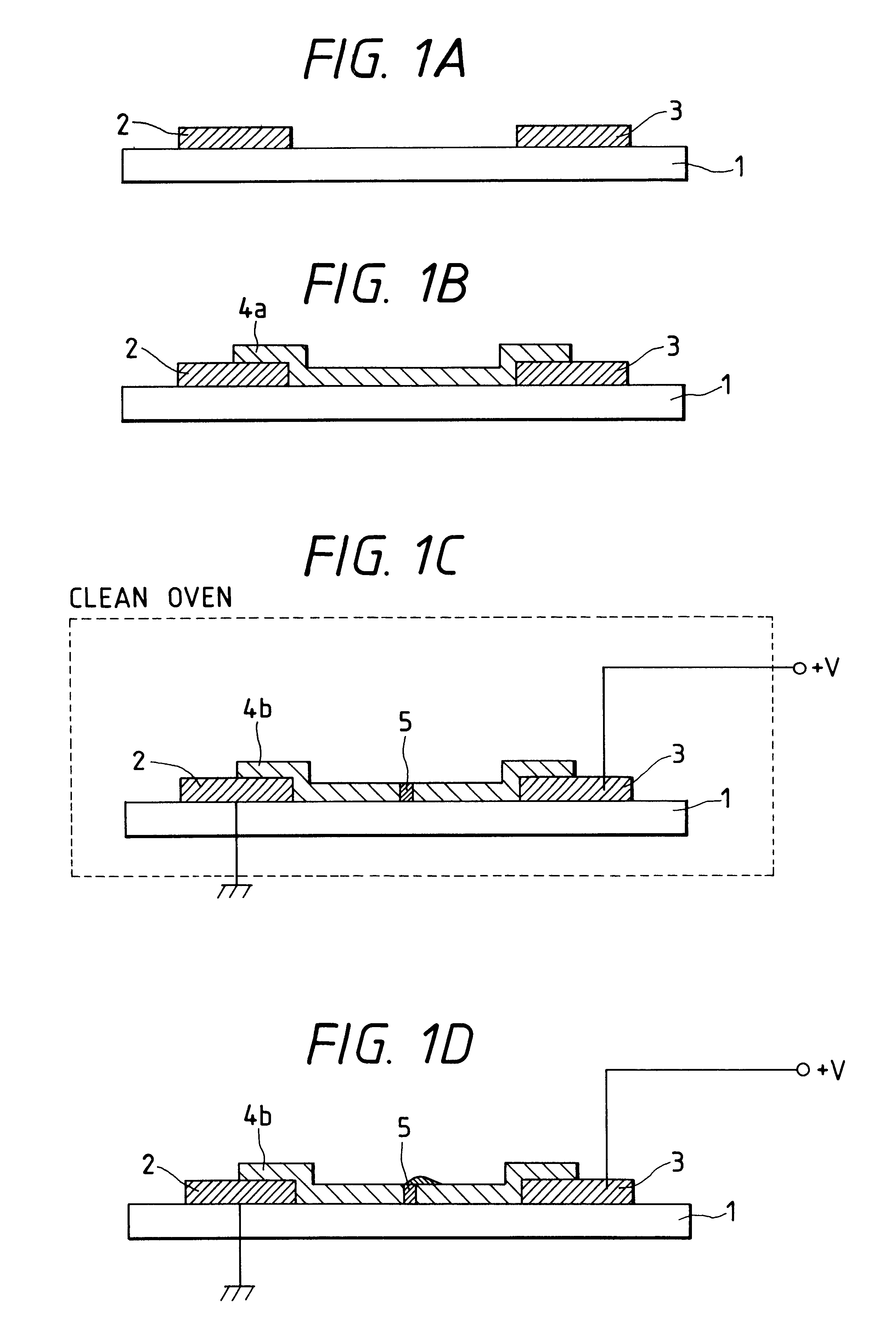
In this example, the process of Step-a of Example 1 was followed to prepare a pair of device electrodes 2 and 3 on a substrate 1.
Step-b)
An organic metal film 4a was formed on the substrate carrying thereon the device electrodes 2 and 3 in a manner as described below.
1 g of ethylene glycol, 0.005 g of polyvinylalcohol and 25 g of IPA were added to 3.2 g of palladium acetate monoethanolamine to prepare 100 g of an aqueous solution thereof, the balance being water. The solution was then applied to a desired location, or the location indicated in FIG. 1B, by means of a bubble-jet type ink-jet apparatus (utilizing part of BJ-10V available from Canon Inc.). For comparison, an organic Pd film was formed on a quartz substrate and dried under the same conditions and thereafter this specimen was tested for the sheet resistance, which was found too high to be measured by the test although obviously it was at least greater than 10.sup.8 .OMEGA. / .quadrature.. Another specimen was prepared under ...
example 3
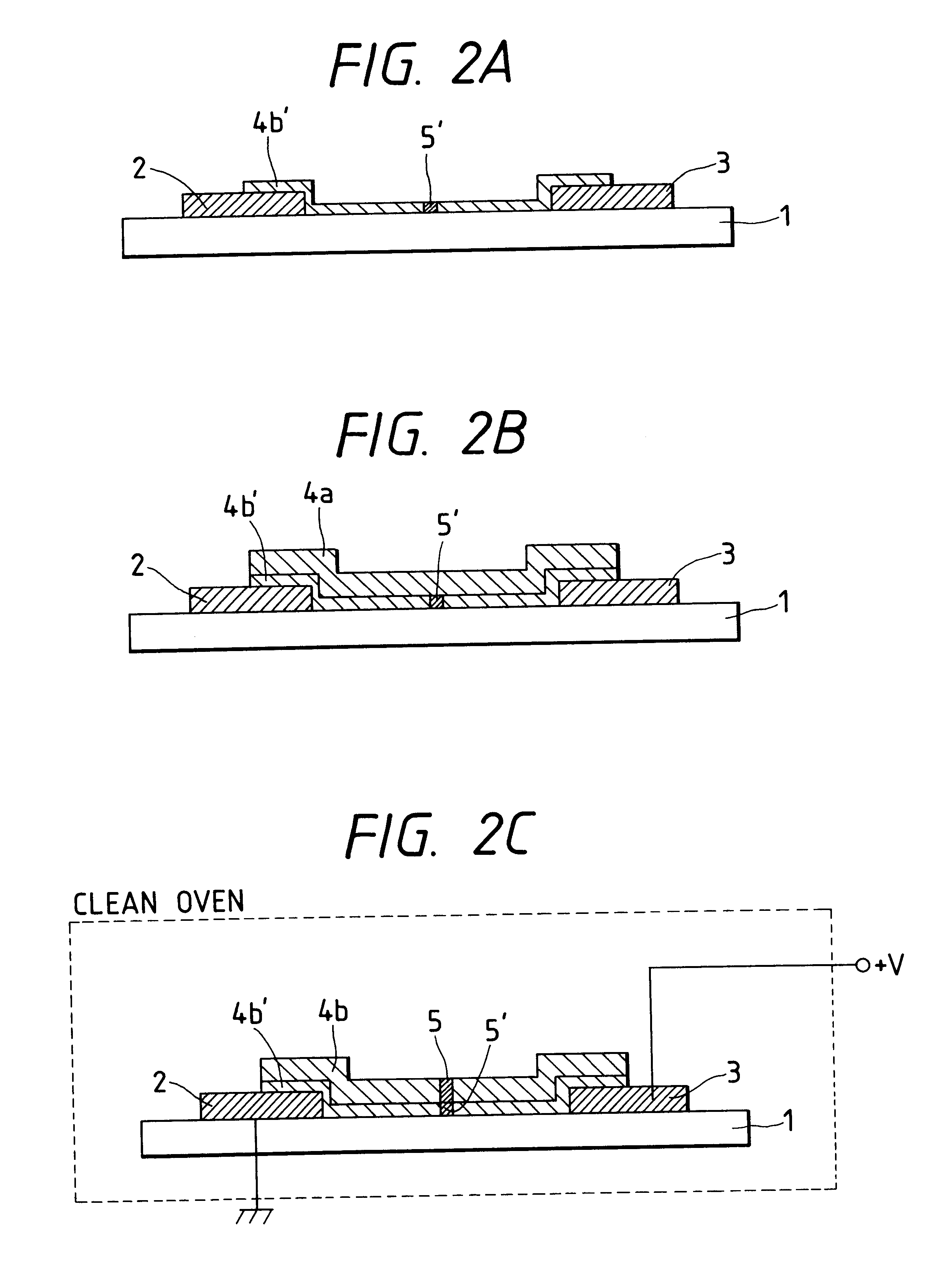
The method used in the example to prepare a surface conduction electron-emitting device is essentially same as the one described earlier by referring to FIGS. 1A, 1B, 2A, 2B and 2C.
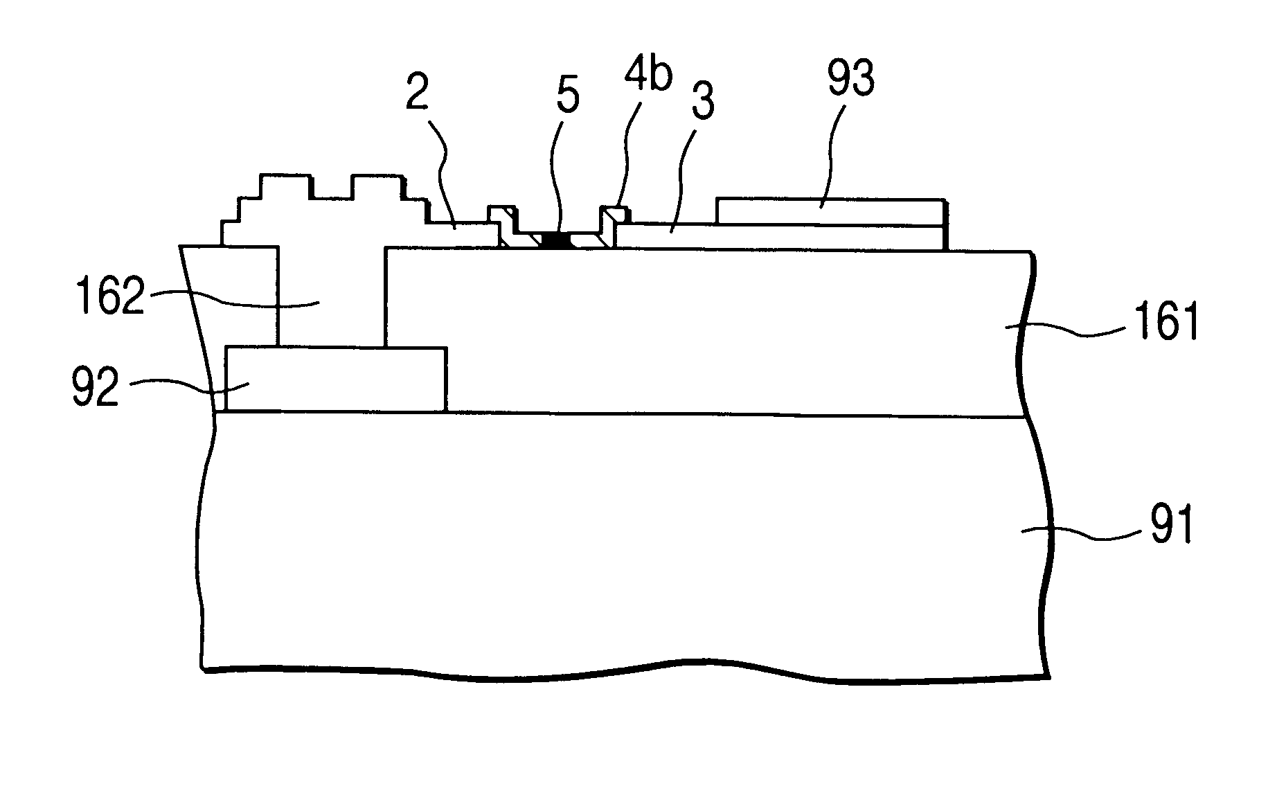
The basic configuration of the device and the method employed for manufacturing it in the example will be described specifically below by referring to FIGS. 1A, 1B, 2A, 2B and 2C. There are shown a substrate 1, a pair of device electrodes 2 and 3, an organic metal film 4a, a second electroconductive film 4b obtained by decomposing the organic metal film 4a, a first electroconductive film 4b', an electron-emitting region 5 formed in the second electroconductive film and a gap 5' produced in the first electroconductive film.
The steps of the manufacturing the device will be described sequentially below also by referring to FIGS. 1A, 1B, 2A, 2B and 2C.
Step-a)
Step-a of Example 1 was followed in this example.
Step-b)
A Cr film was deposited by vacuum evaporation to a thickness of 0.1 .mu.m on the substrate 1 carr...
example 4
In this example, the process of Step-a of Example 1 was followed to prepare a pair of device electrodes 2 and 3 on a substrate 1.
Step-b)
Subsequently, a dichloromethane solution of dodecacarbonyltetrairidium was applied onto a cleansed substrate by means of a spinner, while rotating the substrate. For comparison, a film of the Ir compound was formed on a quartz substrate and dried under the same conditions and thereafter this specimen was tested for the sheet resistance, which was found too high to be measured by the test although obviously it was at least greater than 10.sup.8 .OMEGA. / .quadrature.. Another specimen was prepared under the same conditions and thereafter baked at 300.degree. C. for 10 minutes to find that the formed film contained Ir as the principal ingredient and had a film thickness of 5 nm and a sheet resistance of 1.times.10.sup.4 .OMEGA. / .quadrature..
The sheet resistance of the film of this example slightly rose when the sheet resistance of the film was measured ...
PUM
 Abstract
Description
Claims
Application Information