Silicide block bounded device

a bounded device and silicon block technology, applied in the direction of semiconductor devices, basic electric elements, electrical equipment, etc., can solve the problems of parasitic leakage paths, relatively short paths, leakage paths,

Inactive Publication Date: 2002-01-15
IBM CORP
View PDF6 Cites 26 Cited by
  • Summary
  • Abstract
  • Description
  • Claims
  • Application Information

AI Technical Summary

Problems solved by technology

Parasitic leakage paths have been known to occur in contemporary CMOS technologies which employ field effect transistors that are adjacent or bounded by trenches.
More specifically, it has been found that parasitic leakage results when a divot or recess or both is formed at the interface between the STI oxide region and the Source / Drain (S / D) region (e.g., corner of the SID region adjacent to the STI oxide region).
This brings the silicide closer to the junction between the S / D and STI regions (e.g., at the edge of the S / D region adjacent to the STI region), resulting in a leakage path.
Moreover, a relatively short path for potential leakage may further result when the S / D junction tilts upward at the interface between the S / D region and the STI region, as may occur from depletion or pile-up of the dopant during oxidation steps.
This exposed corner or edge, in turn, brings the silicide closer to the junction between the S / D and STI regions causing leakage at this junction.
However, this reference does not address the placement of a silicide layer which may contribute to the leakage problem, depending on the placement thereof.
However, by using a gate stack for spacing the diode contacts, parasitic capacitance may increase at the S / D region to the polysilicon layer or shorts or other leakage may result, depending on the specific layout of the Voldman, et al. structure.

Method used


Image

  • Silicide block bounded device
  • Silicide block bounded device
  • Silicide block bounded device

Examples


Embodiment Construction

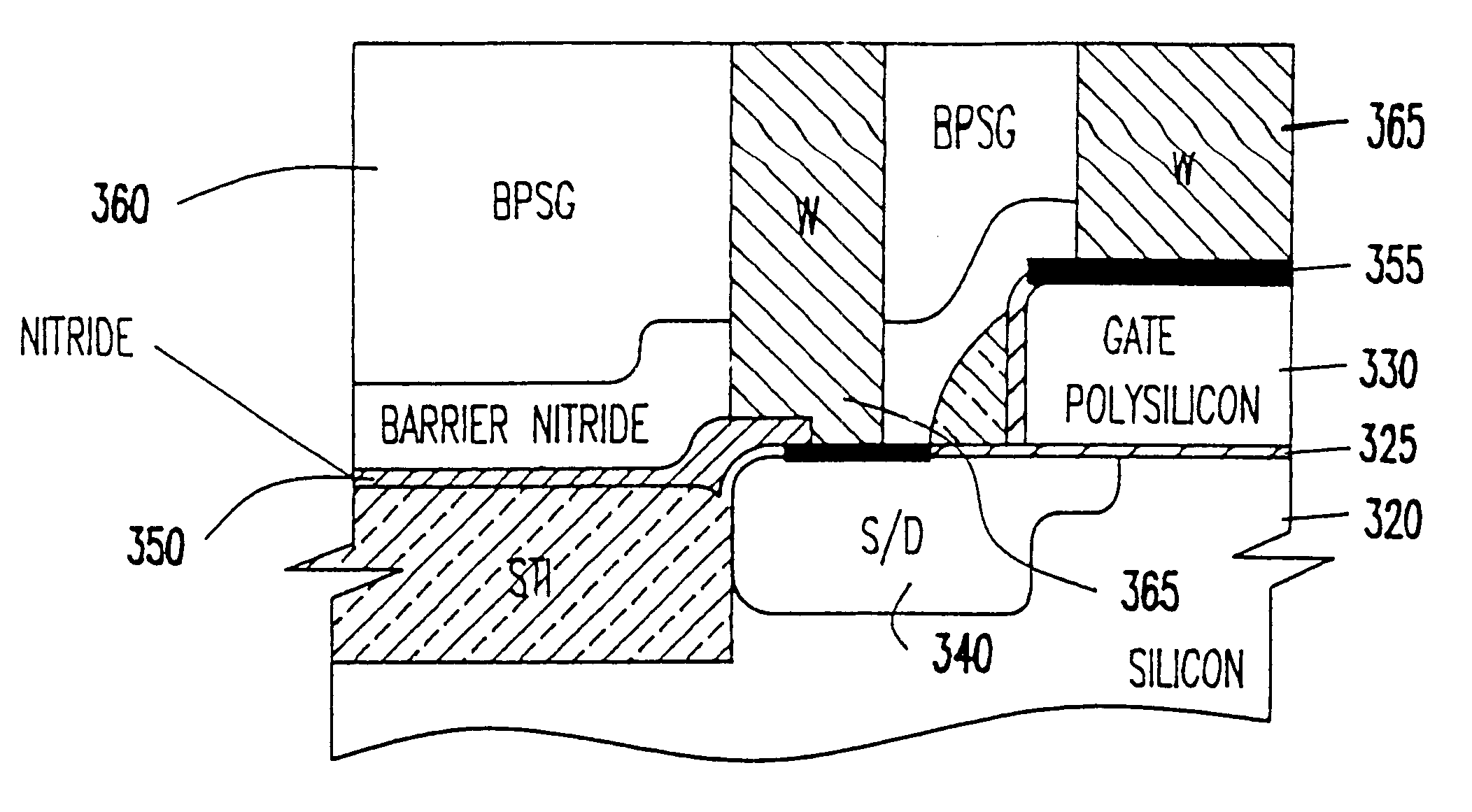
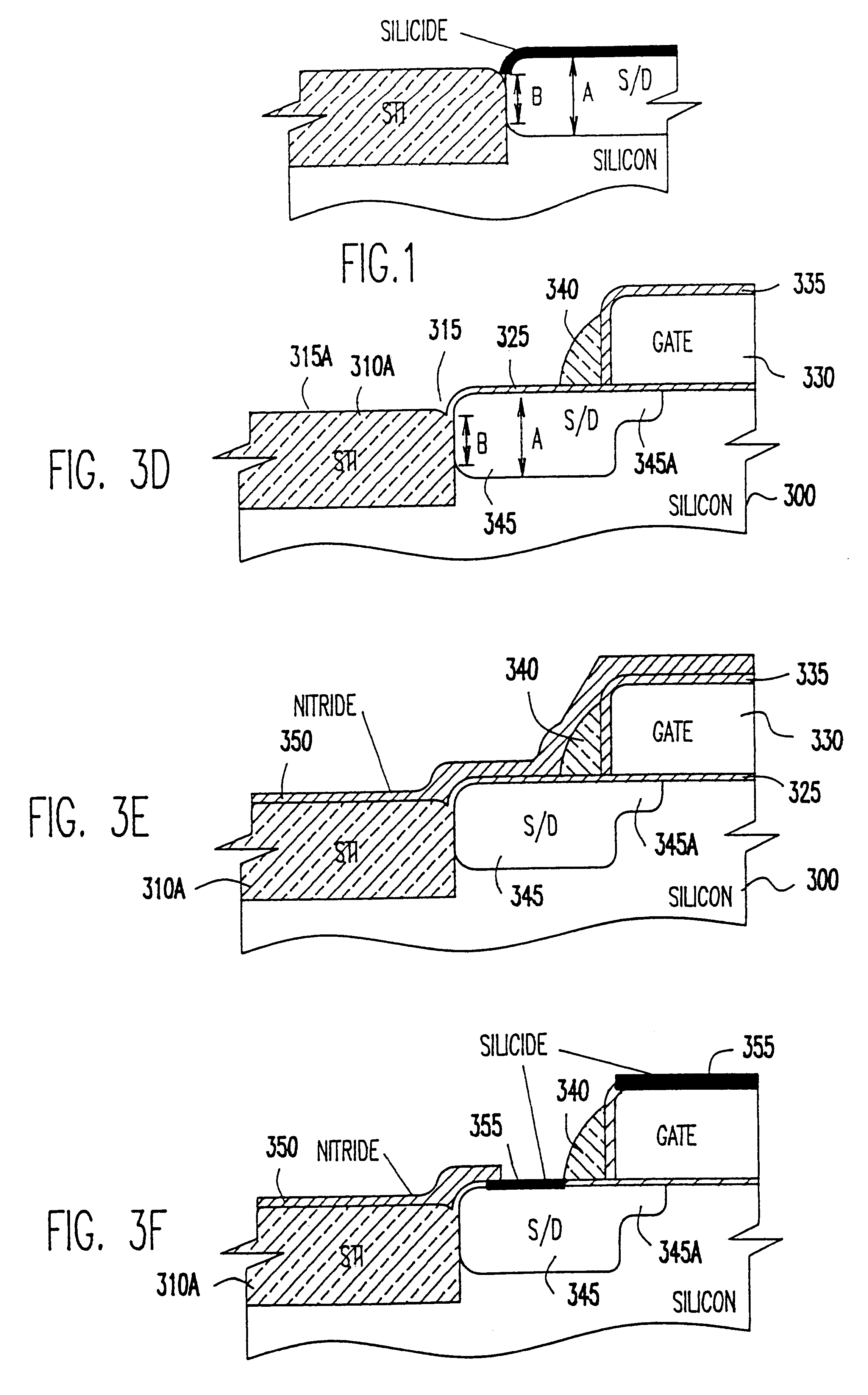
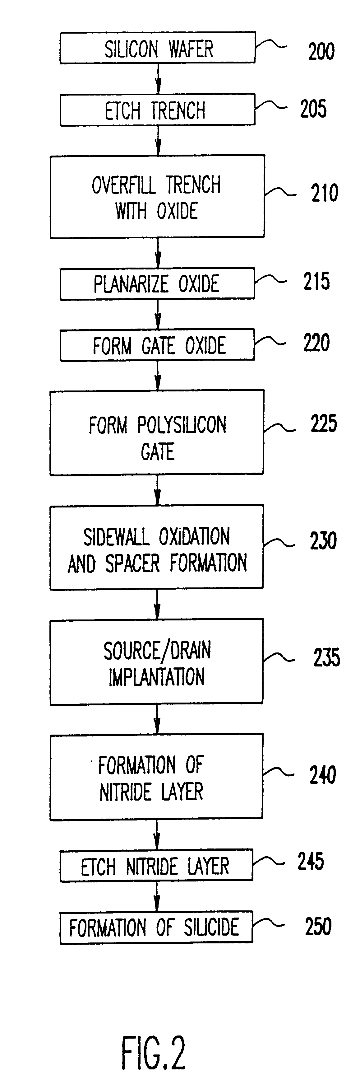
In order to accomplish the objectives of the present invention, a blocking layer is formed at an interface or junction between a first type region and a second type region on a device such as, for example, a Field Effect Transistor (FET). This blocking layer will cover a divot or recess or both that may exist between the interface of the first and second type regions of a conventional FET or other similar device, thereby preventing silicide formation at this interface and any resulting leakage. Referring to at least FIGS. 3d-3f (discussed in more detail below) a divot 315 is formed at the junction of the STI region 310a and the S / D region 345, and a recess 315a is also formed between the STI region and the S / D region (thickness of "B" of the junction depth adjacent to the STI region is less than the thickness of "A" of the S / D region).

Specifically and in the preferred embodiment, the blocking layer is a nitride layer which is etched back so that a landed area is provided over an S / D...


PUM


Abstract

A method and structure for preventing device leakage. The method and structure includes forming a blocking layer of preferably nitride over a junction between a source / drain region and a shallow trench isolation. A silicide is then formed over a landed area of the source / drain region but is blocked by the blocking layer from forming over the junction between the source / drain region and the shallow trench isolation. This prevents device leakage at this location.

Description

1. Field of the InventionThe present invention generally relates to a method and structure for improving device characteristics and, more particularly, to a method and structure for preventing leakage at an interface (junction) formed between a Source / Drain (S / D) region and a shallow trench isolation (STI) region of a Field Effect Transistor (FET) or other similar device.2. Background DescriptionParasitic leakage paths have been known to occur in contemporary CMOS technologies which employ field effect transistors that are adjacent or bounded by trenches. The trenches may be filled with oxide in order to form isolation structures (shallow trench isolation (STI)) or may provide a location for semiconductor devices, such as, for example, capacitors.More specifically, it has been found that parasitic leakage results when a divot or recess or both is formed at the interface between the STI oxide region and the Source / Drain (S / D) region (e.g., corner of the SID region adjacent to the STI...

Claims


Application Information

Patent Timeline
Patent Type & Authority Patents(United States)
IPC IPC(8): H01L21/02H01L21/60H01L21/336
CPCH01L21/76897H01L29/665H01L29/7833
Inventor BALLANTINE, ARNE W.HOOK, TERENCE B.
Owner IBM CORP
Why Eureka
Try Eureka