Semiconductor three-dimensional Hall sensor suitable for high temperature work environment and manufacturing method

A Hall sensor and working environment technology, applied in the direction of instruments, single equipment manufacturing, measuring devices, etc., can solve the problems of multi-dimensional Hall sensor systems, such as bulky, complex chip layout, and failure to work normally, to improve measurement sensitivity, volume Small, good chemical stability effects

Active Publication Date: 2018-04-27
DALIAN UNIV OF TECH
View PDF11 Cites 5 Cited by
  • Summary
  • Abstract
  • Description
  • Claims
  • Application Information

AI Technical Summary

Problems solved by technology

[0013] In order to solve the problems in the prior art that the multi-dimensional Hall sensor system is bulky and the chip layout is complex, resulting in difficult packaging, high cost and failure to work normally in an environment with too high temperature, the present invention provi

Method used


Image

  • Semiconductor three-dimensional Hall sensor suitable for high temperature work environment and manufacturing method
  • Semiconductor three-dimensional Hall sensor suitable for high temperature work environment and manufacturing method
  • Semiconductor three-dimensional Hall sensor suitable for high temperature work environment and manufacturing method

Examples


Embodiment 1

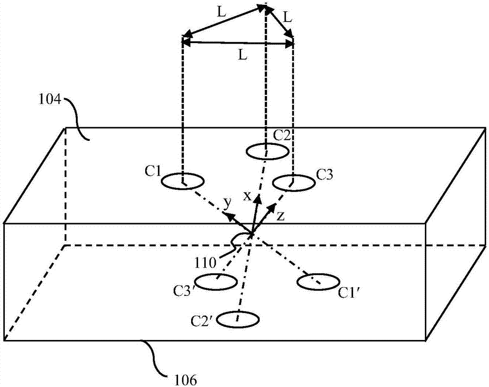
[0044] Such as Figure 4 As shown, wide bandgap semiconductor materials such as SiC or GaN are used, and 5 main electrodes and 8 Hall sensing electrodes are designed and fabricated on the surface of the material, and the metal / semiconductor contact type is ohmic contact. Among them, the 5 main electrodes are 1 central current inflow electrode (B) and 4 current outflow electrodes (B X1 , B X2 , B Z1 and B Z2 ), the 8 Hall sensing electrodes are X 1 ~X 4 and Z 1 ~ Z 4 , where two pairs of Hall sensing electrodes X 1 、X 2 and X 3 、X 4 Measure two magnetic field components in space (X and Z directions), and the remaining four Hall sensing electrodes Z 1 ~ Z 4 Measure the third magnetic field component (Y direction).

[0045] Using insulating layers ①, ②, ③ and ④ embedded between the Hall sensing electrodes, the insulating layer material can be SiO 2 、Si 3 N 4 、Al 2 o 3 etc., using this technology can effectively guide the sensing current direction while significa...

Embodiment 2

[0065] In this embodiment, the intrinsic GaN material is used, and the background carrier concentration of the material is 5×10 15 cm -3 , the insulating layer material used is Si 3 N 4 . The three main electrodes B and B of the device chip X1 , B X2 The size is 40μm×10μm, and the remaining two main electrodes B Z1 , B Z2 The size is 10μm×10μm, Hall sensing electrode Z 1 ~ Z 4 、X 1 ~X 4 The size is 10μm×10μm, the size of each embedded isolation insulating layer is 40μm×60μm, and the Hall sensing electrode X 1 、X 2 The distance between the center and the center of the center main electrode B is 45 μm, and the Hall sensing electrode X 3 、X 4 The distance between the center and the center of the center main electrode B is 30 μm, and the main electrode B Z1 , B Z2 The distance between the center and the center of the center main electrode B is 75 μm, and the main electrode B X1 , B X2 The distance between the center and the center of the center main electrode B is...

Embodiment 3

[0073] As a separate embodiment or as a supplement to Embodiment 1, the central current flowing into the electrode B adopts a circular or rectangular shape; the current flowing out of the electrode B X1 , B X2 , B Z1 , B Z2 The rectangular shape is the preferred choice for both the sensor electrodes and the eight Hall sensing electrodes, and a circular shape can also be used.


PUM


Abstract

The invention discloses a semiconductor three-dimensional Hall sensor suitable for a high temperature work environment and a manufacturing method and belongs to the three-dimensional Hall sensor field. The sensor is characterized in that 5 main electrodes and 8 Hall sensing electrodes are arranged on a semiconductor material surface; the 5 main electrodes include 1 center current inflow electrodeB and 4 current outflow electrodes BX1, BX2, BZ1 and BZ2; the 8 Hall sensing electrodes are Z1 to Z4 and X1 to X4; and insulating layers where the 8 Hall sensing electrodes are embedded are separated.The sensor and the method have advantages that a device leakage current is greatly reduced, a measurement deviation of a device is decreased and device measurement sensitivity is increased; spatial three-dimensional magnetic field detection can be realized in a same semiconductor, and a Hall sensor chip in the scheme has advantages that packaging is simple, the size is small, an energy loss is small and cost is low; the sensor can normally work in an environment where a temperature is higher than 300 DEG C and in various extreme environments of a high temperature, a high voltage, high radiation and the like and can maintain a good linearity.

Description

technical field [0001] The invention belongs to the field of three-dimensional Hall sensors, in particular to a semiconductor three-dimensional Hall sensor suitable for high-temperature working environments and a manufacturing method thereof. Background technique [0002] One-dimensional Hall sensors are divided into horizontal type and vertical type. The typical horizontal type device is cross-shaped, and its structure is as follows figure 1 As shown, there are four identical and symmetrical electrodes C1-C4. An excitation current source is applied to C2 between C1. If there is a magnetic field in the upward direction perpendicular to the device surface, many electrons (assumed to be electrons) move to the direction of electrode C3. At the same time, an equal number of positive charges appear on C4. When they reach stability, the result is between C3 and A Hall potential difference is generated between C4. For the Hall sensor with vertical structure, as described in Docum...

Claims


Application Information

Patent Timeline
IPC IPC(8): G01R33/00G01R33/07
CPCG01R33/0052G01R33/07
Inventor 黄火林曹亚庆孙仲豪李飞雨
Owner DALIAN UNIV OF TECH
Why Eureka
Try Eureka