Method of forming colored film, driving device and liquid crystal display device

a technology of driving device and liquid crystal display device, which is applied in the direction of static indicating device, original photomechanical treatment device, instrument, etc., can solve the problems of high cost, poor light fastness, and difficulty in forming colored films

Inactive Publication Date: 2002-02-05
FUJIFILM BUSINESS INNOVATION CORP
View PDF9 Cites 63 Cited by
  • Summary
  • Abstract
  • Description
  • Claims
  • Application Information

AI Technical Summary

Problems solved by technology

The first dying method requires a photolithographic step for patterning and is poor in light fastness because of the use of a dye and also has a drawback that it requires a number of manufacturing steps.
The second pigment dispersion method also involves a problem of high cost since patterning is conducted by a photolithographic step and a number of steps are required.
The third printing method and the fourth inkjet method require no photolithographic step but the former is poor in the resolution power and the uniformness of the film thickness, while the latter tends to cause color mixing between adjacent filter layers and is poor in view of the resolution power and the positional accuracy.
The fifth electrodeposition method involves a drawback that it requires a patterning step by photolithography such as for forming a common electrode, so that the shape of the pattern is limited and it cannot be used for liquid crystals having TFT.
Further, color filters for liquid crystals cannot generally be used by merely forming a color filter layer and portions between filter cells of respective colors have to be covered with a black matrix, and a photolithographic process is used usually also for the formation of the black matrix, which is one of major factors of cost increase.
By the way, since the liquid crystal display device g

Method used


Image

  • Method of forming colored film, driving device and liquid crystal display device
  • Method of forming colored film, driving device and liquid crystal display device
  • Method of forming colored film, driving device and liquid crystal display device

Examples


second embodiment

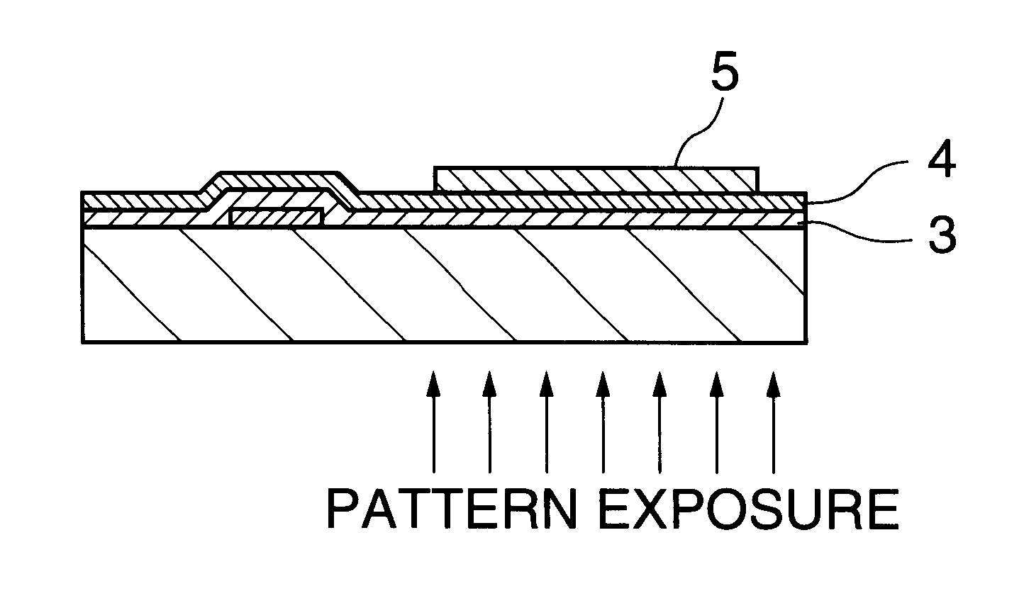
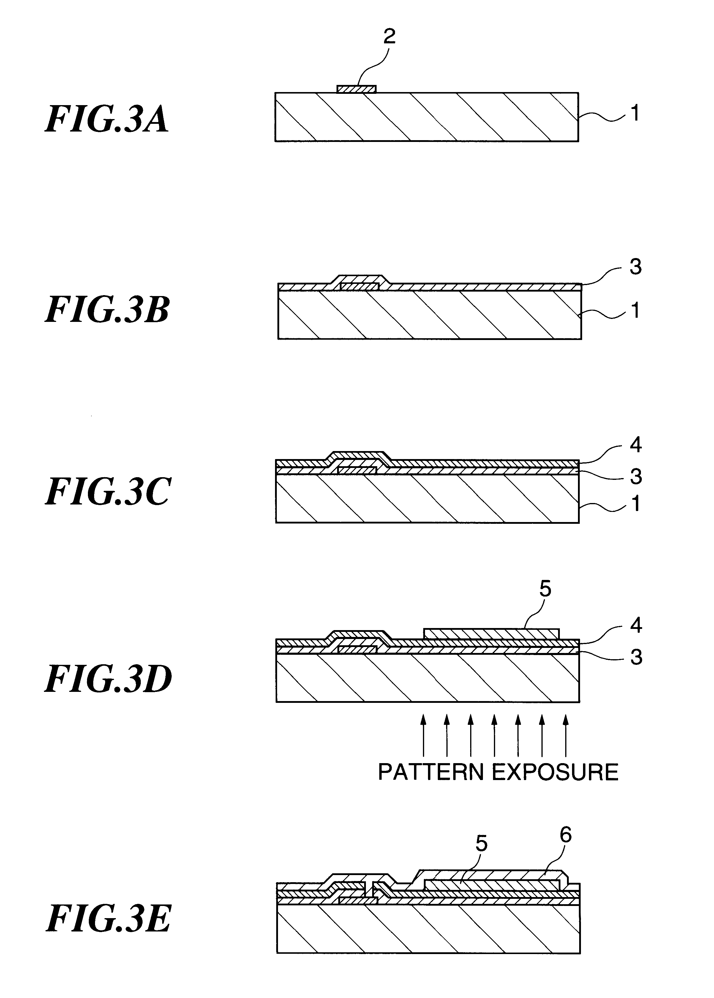
The constitution for the driving device according to the present invention is determined depending on the constitution of the substrate and the constitution of the conductive film and the thin photosemiconductor film to be formed but there is no other particular restrictions and it may be a constitution shown, for example, in FIG. 3D and FIG. 3E, FIG. 4D and FIG. 4E, FIG. 5B and FIG. 7B, in which electronic circuit material (active element) is disposed in the first or The substrate may be of any constitution, and can be properly selected from commercially available substrates or selected properly from the substrates as described previously.

first embodiment

The driving device of the first embodiment is a driving device with a colored film in which a conductive film and a thin photosemiconductor film are laminated in this order on a substrate having an active element with a source electrode, a drain electrode and a gate electrode, the conductive film is electrically connected with the drain electrode and, further, a colored film is electrodeposited on the thin photosemiconductor film to be in contact with the electrolyte by the method of forming the colored film according to the present invention as described previously.

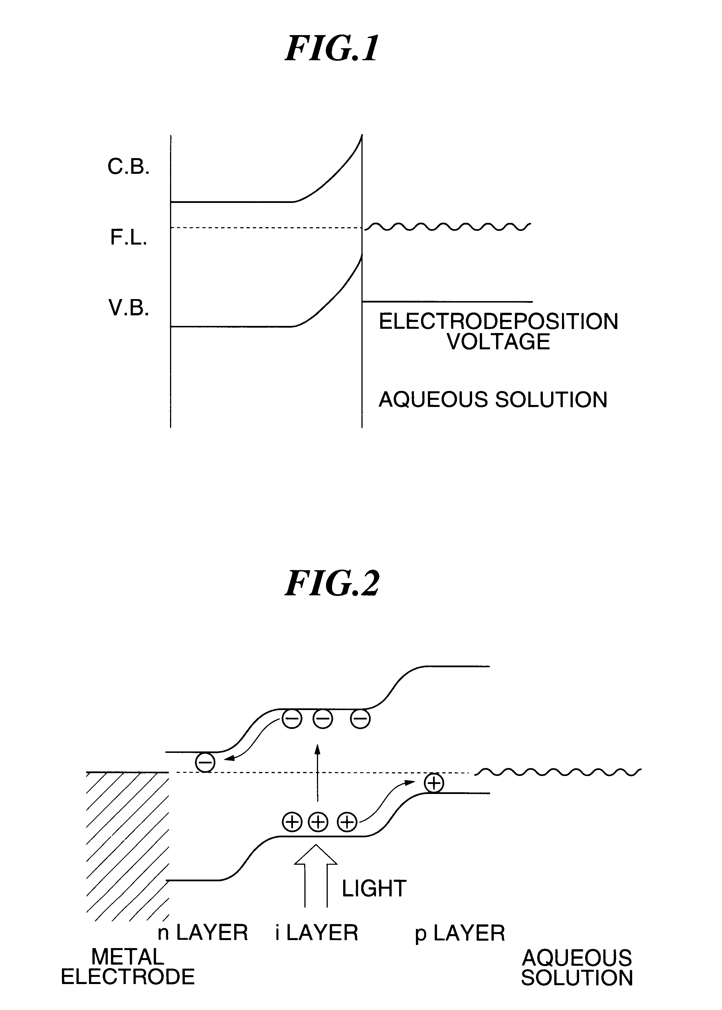
The driving device of the second embodiment is a driving device with a colored film in which thin film transistors as the active element each having a source electrode, a drain electrode and a gate electrode are arranged in a two-dimensional matrix together with the conductive film adjacent with the thin film transistors and, further, the gate electrodes are connected with the first common electrode, the source electrode...

example 1

Electrodeposition Substrate Forming Step

A thin film transistor (TFT) was disposed on one surface of an alkaliless glass support of 0.9 mm in thickness and a transparent conductive film made of a ITO (thin ITO film) of 0.1 .mu.m in thickness was formed by a sputtering method on the identical surface of the substrate adjacent with the drain electrode constituting TFT in a region not formed with the TFT to prepare a substrate having an identical cross sectional structure with that shown in FIG. 4B. The TFT 2 and the thin ITO film 3 are connected by way of a conduction channel 7, that is, a drain electrode constituting the TFT 2. Then, a TiO.sub.2 film (thin TiO.sub.2 film) of 0.2 .mu.m in thickness was formed by a sputtering method on the entire surface of the glass support 1 so as to cover the TFT 2 and the thin ITO film 3 to obtain an electrodeposition substrate of a structure shown in FIG. 4C.

For improving the current characteristic of the thin TiO.sub.2 film on the electrodepositio...


PUM

PropertyMeasurementUnit
Fractionaaaaaaaaaa
Fractionaaaaaaaaaa
Angleaaaaaaaaaa

Abstract

A method of forming a colored film includes a step of forming a substrate for electrodeposition by laminating at least a transparent conductive film and a thin transparent photosemiconductor film having a photovoltaic function in this order on the surface of a support having an electronic circuit materialthereon, and a step of irradiating with a light at least a thin photosemiconductor film of the substrate for electrodeposition while bringing the same into contact with an aqueous electrolyte containing an electrodeposition material containing a colorant, thereby selectively generating a photoelectromotive force to an irradiated area of the thin photosemiconductor film and electrochemically depositing the electrodeposition material to form a colored electrodeposition film; an electronic driving device containing the colored film and a liquid crystal display device having the electronic driving device, the method capable of forming the colored film of high quality and excellent surface smoothness being formed directly on a substrate having thin film transistor and capable of providing a high quality electronic driving device and a liquid crystal display device at low cost.

Description

1. Field of the InventionThe present invention concerns a method of forming a colored film, a driving device a and liquid crystal display device and, more particularly, it relates to a method of forming a colored film (color filter film) directly to a substrate having an active elements such as a thin film transistor (TFT), a driving device including the colored film and a liquid crystal display device having the driving device.2. Description of the Related ArtAt present, known manufacturing methods for color filters include, for example, (1) a dying method, (2) a pigment dispersing method, (3) a printing method, (4) an ink jet method and (5) an electrodeposition method, which have inherent features and advantages respectively but involve the following drawbacks:The first dying method requires a photolithographic step for patterning and is poor in light fastness because of the use of a dye and also has a drawback that it requires a number of manufacturing steps.The second pigment di...

Claims


Application Information

Patent Timeline
IPC IPC(8): C25D13/04G02F1/1335G02F1/13G02B5/20G02F1/136G02F1/1368
CPCC25D13/04G02B5/201G02F1/133516G02F2202/12G02F2202/10
Inventor AKUTSU, EIICHIOHTSU, SHIGEMITOMONO, TAKAOSHIMIZU, KEISHI
Owner FUJIFILM BUSINESS INNOVATION CORP
Why Eureka
Try Eureka