Method for forming an L-shaped spacer using a disposable polysilicon spacer

a technology of polysilicon and spacer, which is applied in the manufacturing of semiconductor/solid-state devices, electrical devices, transistors, etc., can solve the problems of affecting the shape and size of the spacer, the top oxide portion of the spacer cannot be easily removed without damaging the oxide isolation structure, and the spacer shape and size is inconsistent across the ic and between the i

Inactive Publication Date: 2002-02-12
CHARTERED SEMICONDUCTOR MANUFACTURING
View PDF7 Cites 40 Cited by
  • Summary
  • Abstract
  • Description
  • Claims
  • Application Information

AI Technical Summary

Problems solved by technology

The reduced space between gate electrodes can cause poor gap fill by the subsequent dielectric layer (eg inter-layer dielectric) resulting in degraded performance.
However, the top oxide portion of the spacer can not be easily removed without damaging oxide isolation structures.
Conversly, if the top oxide portion of the spacer remains, it can be effected by post-etch wet chemical process causing inconsistent spacer shape and size across the IC and between IC's.
Also, the gap filling ability of the subsequent dielectric layer is not optimized, because the aspect ratio remains high due to the presence of the oxide portion of the spacers.
Another problem with conventional L-shaped spacers is that dry etching nitride spacers can result in variations in spacer width between isolated areas and areas nested between adjacent gates.
These variations in spacer width will cause un

Method used


Image

  • Method for forming an L-shaped spacer using a disposable polysilicon spacer
  • Method for forming an L-shaped spacer using a disposable polysilicon spacer
  • Method for forming an L-shaped spacer using a disposable polysilicon spacer

Examples


Embodiment Construction

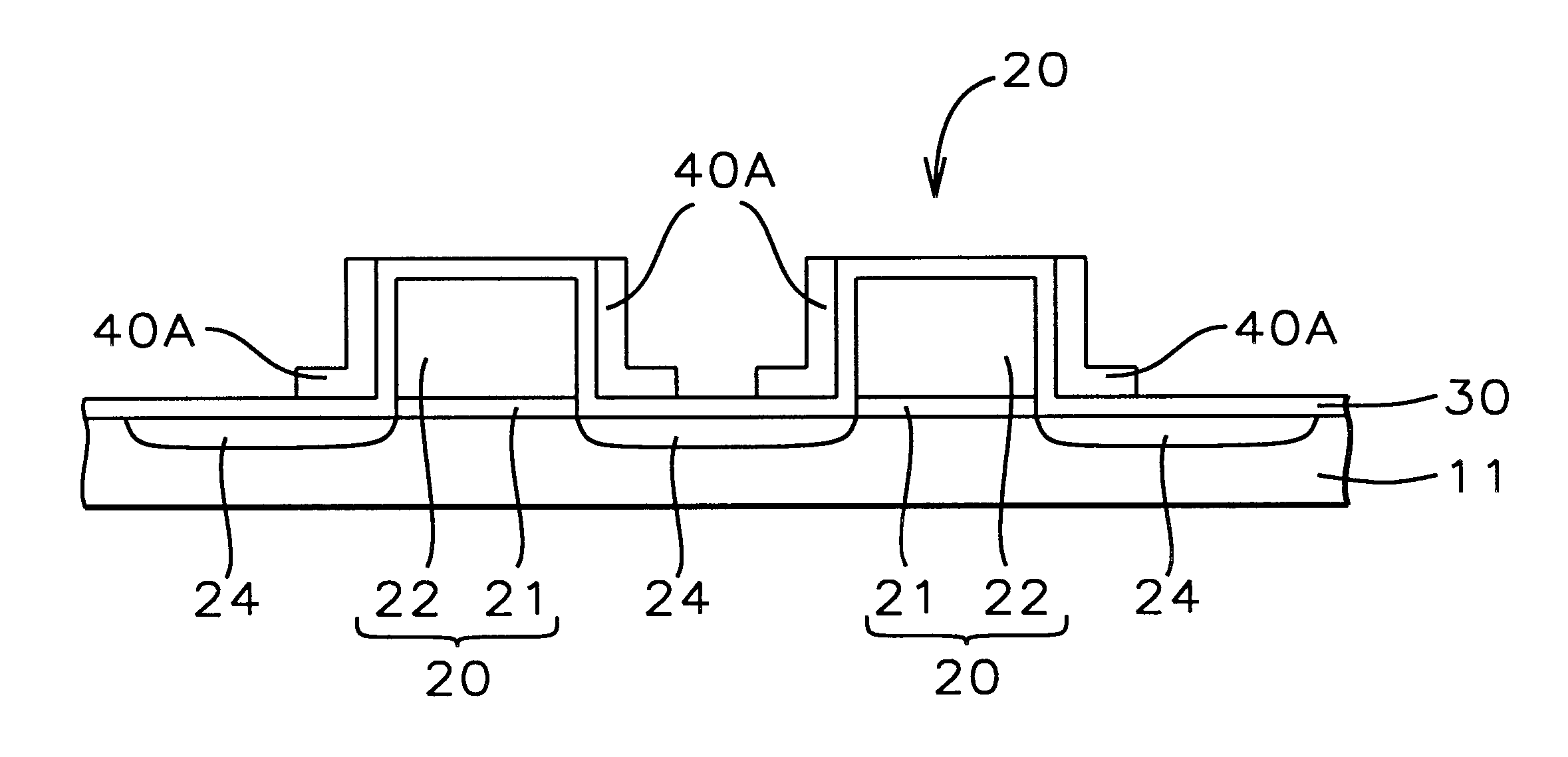
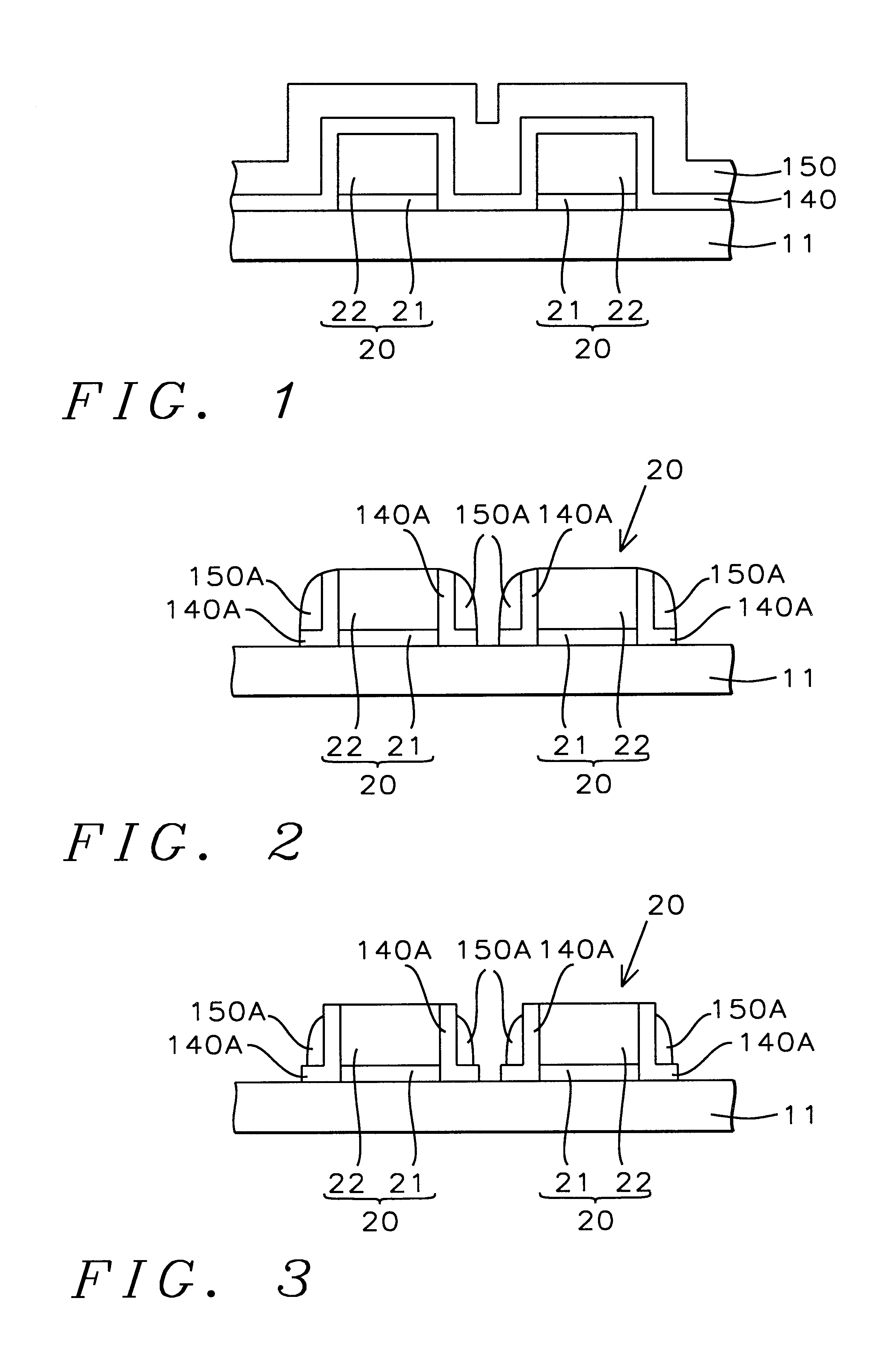
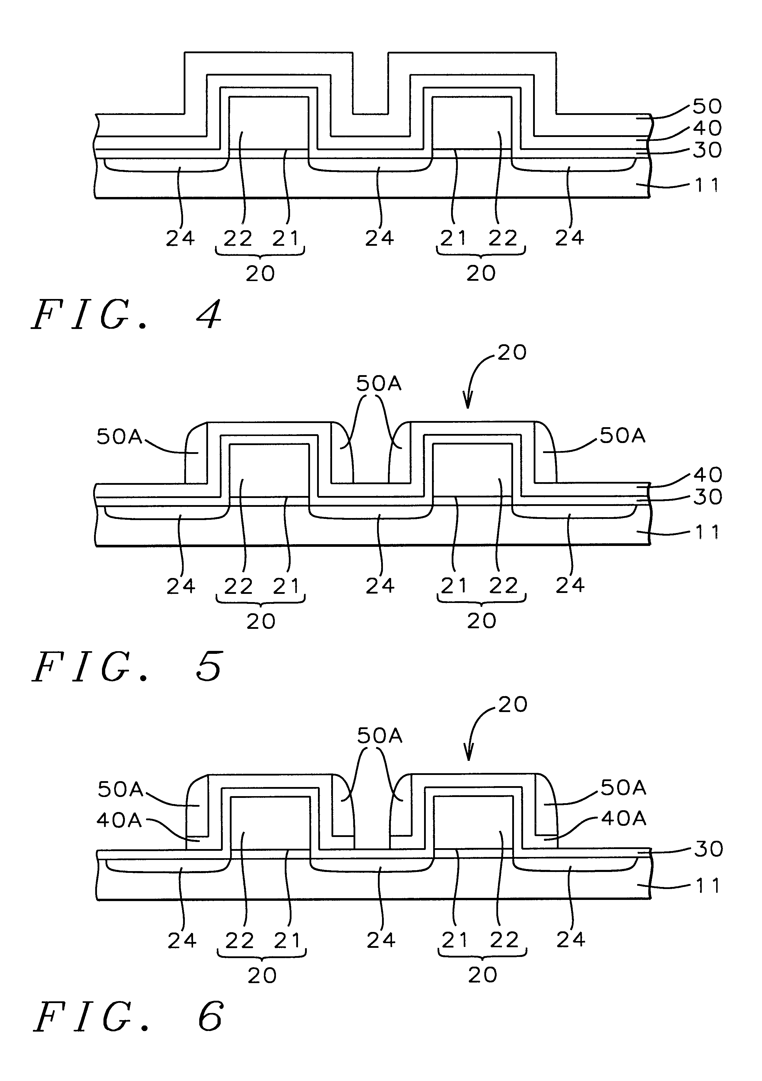
A preferred embodiment of the present invention is described with reference to FIGS. 4 through 7. The preferred embodiment provides a method for forming an L-shaped spacer using a disposable polysilicon top spacer. The present invention provides a consistently controllable opening which is adequate for good gap-filling characteristics. Also, the present invention provides uniform L-shaped spacers, resulting in symmetrical transistors.

Referring to FIG. 4, the preferred embodiment of the present invention begins by providing a semiconductor structure (11). Semiconductor substrate (11) is understood to possibly include a substrate comprising a wafer of semiconductor material such as silicon or germanium or a like substrate structure such as silicon-on-insulator (SOI) as is known in the art. Semiconductor structure (11) should be understood to possibly further include one or more conductive and / or insulating layers and passive and / or active devices formed on or over said substrate. The ...


PUM


Abstract

A method for forming an L-shaped spacer using disposable polysilicon top spacers. A semiconductor structure is provided having a gate structure thereon. A liner oxide layer is formed on the gate structure. A dielectric spacer layer is formed on the liner oxide layer. A disposable polysilicon top spacer layer is formed on the dielectric spacer layer. The disposable polysilicon top spacer layer is anisotropically etched to form disposable polysilicon top spacers. The dielectric spacer layer is etched to form L-shaped dielectric spacers, using the disposable polysilicon top spacers as an etch mask. The disposable polysilicon top spacers are removed leaving an L-shaped dielectric spacer. In one embodiment, lightly doped source and drain regions are formed prior to forming the liner oxide layer and the L-shaped spacers.

Description

BACKGROUND OF INVENTION1) Field of the inventionThis invention relates generally to fabrication of a semiconductor device and more particularly to a method for forming an L-shaped spacer using a disposable polysilicon top spacer.2) Description of the Prior ArtAs the physical geometry of semiconductors continues to shrink, the space between gate electrodes shrinks as well. The reduced space between gate electrodes can cause poor gap fill by the subsequent dielectric layer (eg inter-layer dielectric) resulting in degraded performance.One approach which has been used to solve this problem is the use of spacers on the gate electrode sidewalls which are smaller at the top than they are at the bottom, such as L-shaped spacers. In a typical L-shaped spacer two dielectric layers (the first composed of silicon nitride and the second composed of silicon oxide) are formed over and around a gate electrode, then anisotropically etched. However, the top oxide portion of the spacer can not be easi...

Claims


Application Information

Patent Timeline
IPC IPC(8): H01L21/02H01L21/336H01L21/3213
CPCH01L21/32137H01L29/6659H01L29/6653
Inventor PRADEEP, YELEHANKA RAMACHANDRAMURTHYGUPTA, SUBHASHCHHAGAN, VIJAI KOMAR
Owner CHARTERED SEMICONDUCTOR MANUFACTURING
Why Eureka
Try Eureka