Production of silicon carbide bodies

Inactive Publication Date: 2002-04-02
NGK INSULATORS LTD
View PDF5 Cites 3 Cited by
  • Summary
  • Abstract
  • Description
  • Claims
  • Application Information

AI Technical Summary

Benefits of technology

It is an object of the present invention to remarkably increase the electric res

Problems solved by technology

Such silicon carbide bodies are dense and highly corrosion resistive.
However, although producing conditions for carrying out the chemical vapor deposition such as a carrier gas flow rate, a silicon source gas flow rate,

Method used


Image

  • Production of silicon carbide bodies
  • Production of silicon carbide bodies

Examples


Example

EXAMPLE

A silicon carbide mass was formed on a surface of a substrate by chemical vapor deposition. As the substrate, a discoid substrate made of graphite, 100 mm in diameter and 10 mm in thickness was used. Argon was fed as a carrier gas during when the temperature rose. Then, hydrogen was first flown for 10 minutes, then silicon tetrachloride was flown for 1 minutes, and thereafter silicon tetrachloride and methane were introduced. The flow rate of each gas at the film-forming temperature was as follows:

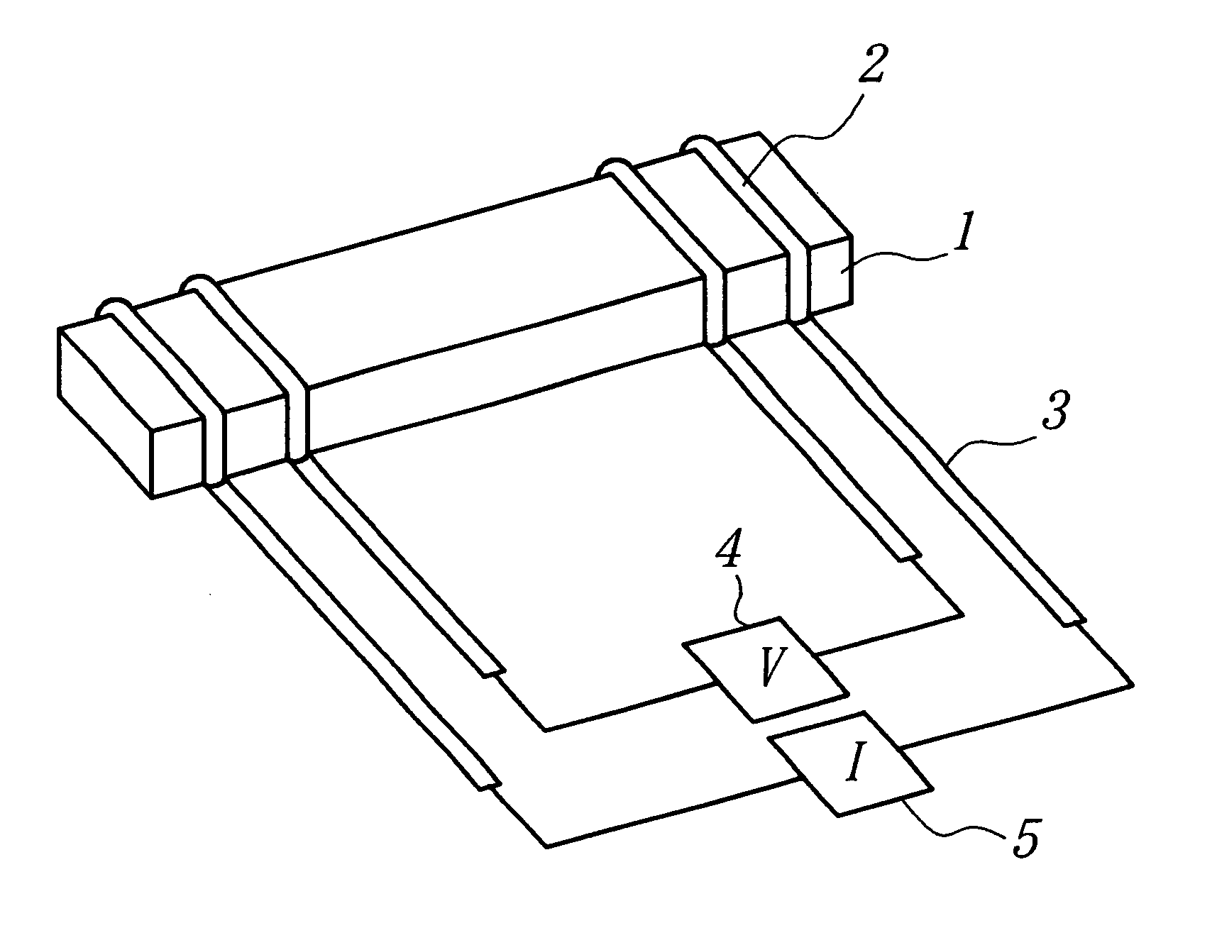
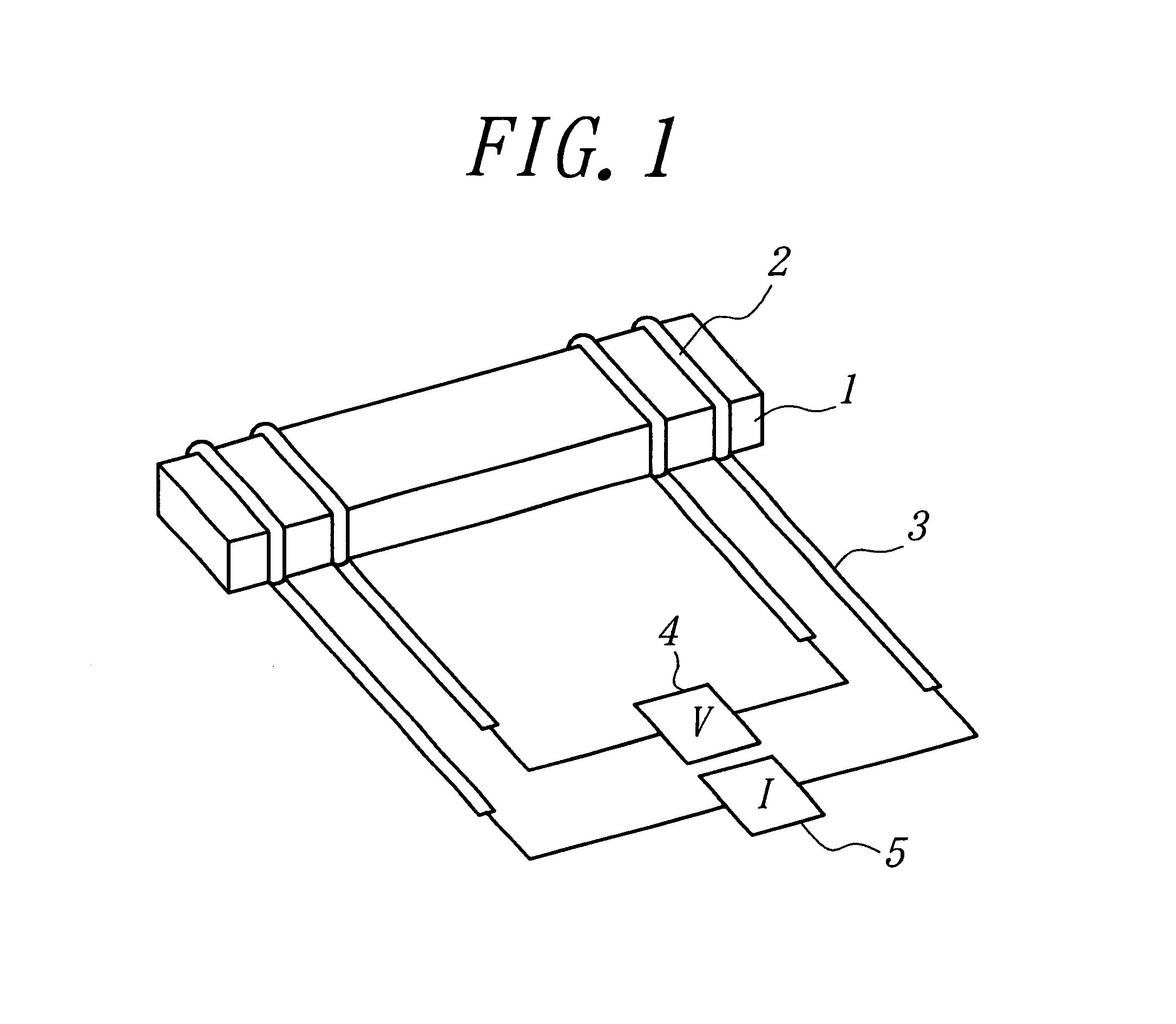
Silicon carbide bodies A, B and C were produced in this manner. Each of the silicon carbide bodies had a thickness of 3 to 5 mm. Then, with respect to each of the silicon carbide bodies A, B, and C, only the silicon carbide body was removed from the substrate, and a plurality of samples 1 as shown in FIG. 1, 4 mm wide, 2 mm thick and 40 mm long, were obtained. The samples correspond to A-1 to A-7, B-1 to B-6 and C-1 to C-6 in FIGS. 1 to 3. With respect to each sample, the electrical...


PUM

PropertyMeasurementUnit
Fractionaaaaaaaaaa
Fractionaaaaaaaaaa
Timeaaaaaaaaaa

Abstract

A method for producing a silicon carbide body, includes the steps of forming a silicon carbide mass by chemical vapor deposition, and thermally treating the silicon carbide mass under vacuum or in an inert gas atmosphere at a temperature not less than 2000.degree. C., the silicon carbide article having an electric resistivity higher than that of the silicon carbide mass having not been thermally treated.

Description

BACKGROUND OF THE INVENTION(1) Field of the InventionThe present invention relates to a method for producing silicon carbide articles.(2) Related Art StatementFor example, JP-A-10-256,108 and JP-A-01-224,286 describe methods for producing silicon carbide bodies on surfaces of substrates of such as graphite by chemical vapor deposition. Such silicon carbide bodies are dense and highly corrosion resistive.The inventors have urgently needed to increase the electric resistivity of silicon carbide bodies and obtain such silicon carbide bodies having high resistivities. For, the formation of highly resistive silicon carbide bodies have been demanded in the field of the semiconductor-producing apparatuses. However, although producing conditions for carrying out the chemical vapor deposition such as a carrier gas flow rate, a silicon source gas flow rate, a carbon source gas flow rate, a film-forming temperature and a film forming time were changed in various ways, it was difficult to incre...

Claims


Application Information

Patent Timeline
IPC IPC(8): C23C16/56C23C16/32
CPCC23C16/56C23C16/325
Inventor YAMADA, HIROTAKEMURAI, MAKOTOFURUKUBO, HIROSHIAIHARA, YASUFUMIOHASHI, TSUNEAKI
Owner NGK INSULATORS LTD
Why Eureka
Try Eureka