Gallium nitride group semiconductor laser device and optical pickup apparatus

a technology of gallium nitride and laser device, which is applied in the direction of lasers, optical beam sources, semiconductor lasers, etc., can solve the problems of affecting the intensity of the output light of the semiconductor laser device, and no layer for absorbing laser light formation

Inactive Publication Date: 2002-04-09
SURFWAX +1
View PDF4 Cites 47 Cited by
  • Summary
  • Abstract
  • Description
  • Claims
  • Application Information

AI Technical Summary

Problems solved by technology

As a result, the interference of output light from the semiconductor laser device decreases.
Further, no layer for absorbing laser light is formed between the active layer and the substrate.
It has been found, therefore, that an interference pattern formed by the return beam at the illumination position B and the laser light in the active region interact with each other, resulting in influencing the intensity of the output light of the semiconductor laser device.
If the intensity of the output light varies, such a semiconductor laser device is not practically usable as a light source of an optical disk syst...

Method used


Image

  • Gallium nitride group semiconductor laser device and optical pickup apparatus
  • Gallium nitride group semiconductor laser device and optical pickup apparatus
  • Gallium nitride group semiconductor laser device and optical pickup apparatus

Examples


example 2

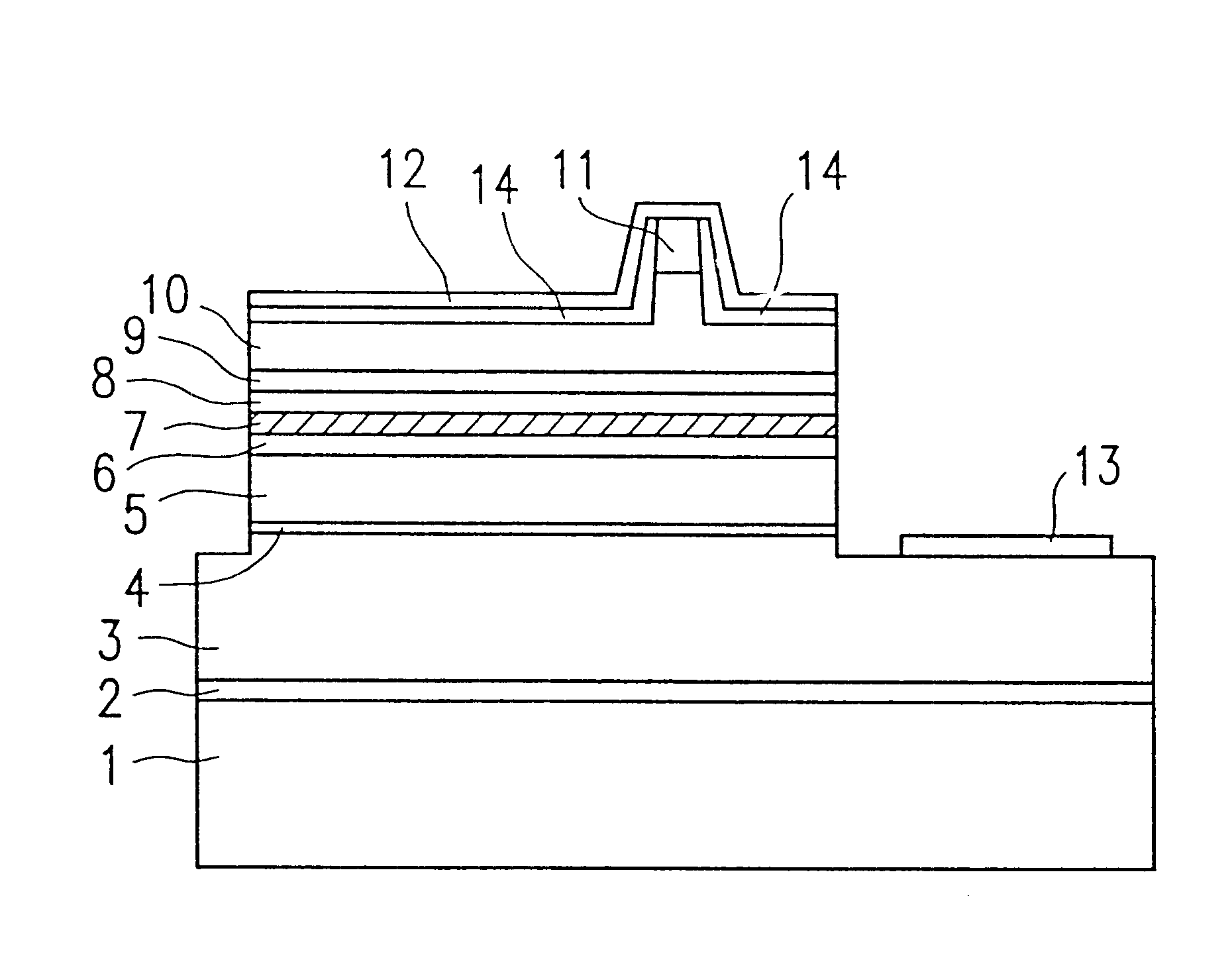
A GaN semiconductor laser device of Example 2 according to the present invention is fabricated in the same manner as that in Example 1, except that the light absorption layer is of a MQW structure having a total thickness of 0.065 .mu.m composed of seven Si-doped n-type In.sub.0.2 Ga.sub.0.8 N layers (thickness: 5 nm each) and six Si-doped n-type In.sub.0.03 Ga.sub.0.97 N layers (thickness: 5 nm each), and that an Si-doped n-type Al.sub.0.2 Ga.sub.0.8 N evaporation prevention layer is formed on the light absorption layer at the same growth temperature as that for the light absorption layer.

The thus-fabricated GaN group semiconductor laser device of this example has an oscillation wavelength of 410 nm and an oscillation threshold current of 30 mA, providing good laser characteristics as in Example 1. Since the light absorption layer 4 of the MQW structure is formed, return light incident on the sapphire substrate is blocked from interacting with laser light in the active region. Thus...

example 3

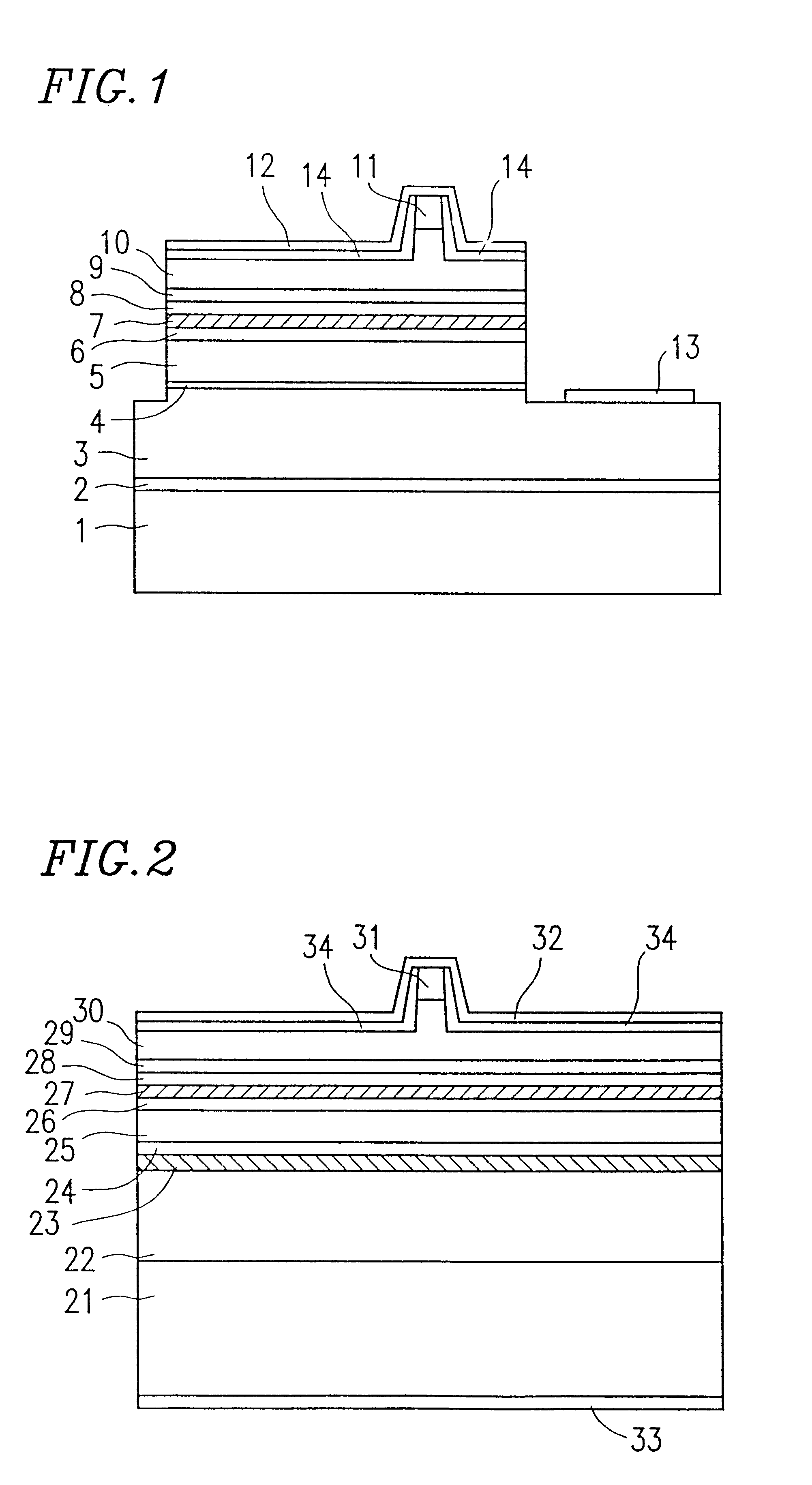
FIG. 2 is a cross-sectional view of a GaN group semiconductor laser device of Example 3 according to the present invention. Referring to FIG. 2, the GaN group semiconductor laser device of Example 3 includes an n-type GaN substrate 21 having a c plane surface, an n-type GaN contact layer 22, a light absorption layer 23 of a MQW structure composed of seven n-type In.sub.0.2 Ga.sub.0.8 N layers and six n-type In.sub.0.03 Ga.sub.0.97 N layers, an n-type Al.sub.0.2 Ga.sub.0.9 N evaporation prevention layer 24, an n-type Al.sub.0.1 Ga.sub.0.9 N cladding layer 25, an n-type GaN guide layer 26, an active layer 27 of a MQW structure composed of three In.sub.0.15 Ga.sub.0.85 N quantum well layers and two In.sub.0.03 Ga.sub.0.97 N barrier layers, an Al.sub.0.2 Ga.sub.0.8 N evaporation prevention layer 28, a p-type GaN guide layer 29, a p-type Al.sub.0.1 Ga.sub.0.9 N cladding layer 30, a p-type GaN contact layer 31, a p-side electrode 32, an n-side electrode 33, and an SiO.sub.2 insulating fil...

example 4

In this example, an optical pickup apparatus employing the three-beam method shown in FIG. 6 is fabricated using the GaN group semiconductor laser device of Example 3 as a light source.

The semiconductor laser device used in this example includes the light absorption layer which blocks return light incident on the n-type GaN substrate from interacting with laser light in the active region. Thus, the semiconductor laser device can provide output light with stable intensity without the influence of return light. Further, since the semiconductor laser device has the self-oscillation property, generation of noise caused by return light directly returning to the active region is suppressed. As a result, when the optical pickup apparatus of this example is used to read data from an optical disk, data read without error is possible.

Optical pickup apparatus which realize data read without error as described above can also be obtained by using the GaN group semiconductor laser devices of Exam...


PUM


Abstract

The gallium nitride group semiconductor laser device of this invention includes an active layer made of a nitride semiconductor formed between cladding layers and/or guide layers made of a nitride semiconductor on a substrate, wherein a light absorption layer is formed between the substrate and one of the cladding layers located closer to the substrate, the light absorption layer being made of a semiconductor having an energy gap substantially equal to or smaller than an energy gap of the active layer.

Description

1. Field of the InventionThe present invention relates to a gallium nitride (GaN) group semiconductor laser device incorporated as a light source in an optical system of an optical pickup apparatus for an optical disk and the like.2. Description of the Related ArtGaN group (GaInAlN) semiconductors are used as materials for semiconductor laser devices having an emission wavelength in a range of ultraviolet to green light wavelengths. A semiconductor laser device using GaN group semiconductors is described in MRS Internet J. Nitride Semiconductor Res. Vol. 2 (1997) Art. 5, for example. FIG. 4 shows a cross-sectional view of this conventional semiconductor laser device. Referring to FIG. 4, the semiconductor laser device includes a sapphire substrate 201, a GaN buffer layer 202, an n-type GaN contact layer 203, an n-type In.sub.0.05 Ga.sub.0.95 N layer 204, an n-type Al.sub.0.08 Ga.sub.0.92 N cladding layer 205, an n-type GaN guide layer 206, an active layer 207 of a multi-quantum well...

Claims


Application Information

Patent Timeline
IPC IPC(8): G11B7/125H01S5/323H01S5/00H01S5/22G11B7/127H01L33/06H01L33/32
CPCG11B7/127H01S5/32341H01S5/2219
Inventor OKUMURA, TOSHIYUKI
Owner SURFWAX
Why Eureka
Try Eureka