Solid-state relay

a solid-state relay and relay technology, applied in the direction of semiconductor devices, semiconductor/solid-state device details, electrical apparatus, etc., can solve the problems of unduly large parallel connected capacitance between the source and the ldmosfet of this structure, and not be satisfactory for minimizing

Inactive Publication Date: 2002-04-16
MATSUSHITA ELECTRIC WORKS LTD
View PDF15 Cites 8 Cited by
  • Summary
  • Abstract
  • Description
  • Claims
  • Application Information

AI Technical Summary

Benefits of technology

Since the well region is diffused over the full depth of the silicon layer to have its bottom abutted against the buried oxide layer, the well region of the second conductive type forms with the silicon layer of the first conductive type a P-N interface only at a small portion adjacent the channel. That is, only a side boundary of the well region laterally confronting the drain region forms the P-N interface. Because of this reduced P-N interface and also because of the buried oxide layer exhibiting much lower capacitance than the silicon layer, it is possible to greatly reduce a drain-source capacitance for minimizing the output capacitance of the relay in the non-conductive condition. Also the reduced P-N interface area can reduce a leak current at the non-conducting condition of the output terminals. Moreover, the SOI structure can assure sufficient flexibility for mounting the LDMOSFET on the supporting plate, either with one of the drain and source being electrically connected to the supporting plate or being electrically isolated, in accordance with particular demands.
In a further version of the present invention, it is contemplated to integrate the two LDMOSFET in a single device structure. In this structure, the well region are formed in the single silicon layer over the full depth thereof in such a manner as to form therein a laterally isolated pair of first and second active zones. Diffused in the well region is a pair of first and second source regions which surround respectively the first and second active zones and define first and second channels extending within the well regions from the first and second source regions to confronting boundaries of the first and second active zones, respectively. First and second drain regions are diffused respectively within the first and second active zone so as to be isolated from each other by the well region. First and second drain electrodes are placed respectively on the first and second drain regions in an electrical connecting relationship therewith. At least one gate electrode is electrically connected to first and second gate layers which are placed over the first and second channels respectively through dielectric layers and define first and second gates of the two LDMOSFETs, respectively. A common source electrode is provided to bridge over the first and second source regions and is electrically connected thereto. The silicon substrate carrying the silicon layer through the buried oxide layer is mounted on the supporting frame with the output terminals being electrically connected respectively to the first and second drains. Thus, the two LDMOSFETs can be realized in the single device structure and can be easily assembled into the solid-state relay, while retaining to minimize drain-source capacitance.

Problems solved by technology

Accordingly, the LDMOSFET of this structure is not satisfactory for minimizing the output capacitance between the output terminals of the relay.
Otherwise, the additional path would add a capacitance in parallel with the secondary drain-source capacitance inevitably developed between the bottom of the well region and the supporting plate through the buried oxide layer, thereby bringing about unduly large parallel connected capacitance between the source and drain.

Method used


Image

  • Solid-state relay
  • Solid-state relay
  • Solid-state relay

Examples


second embodiment

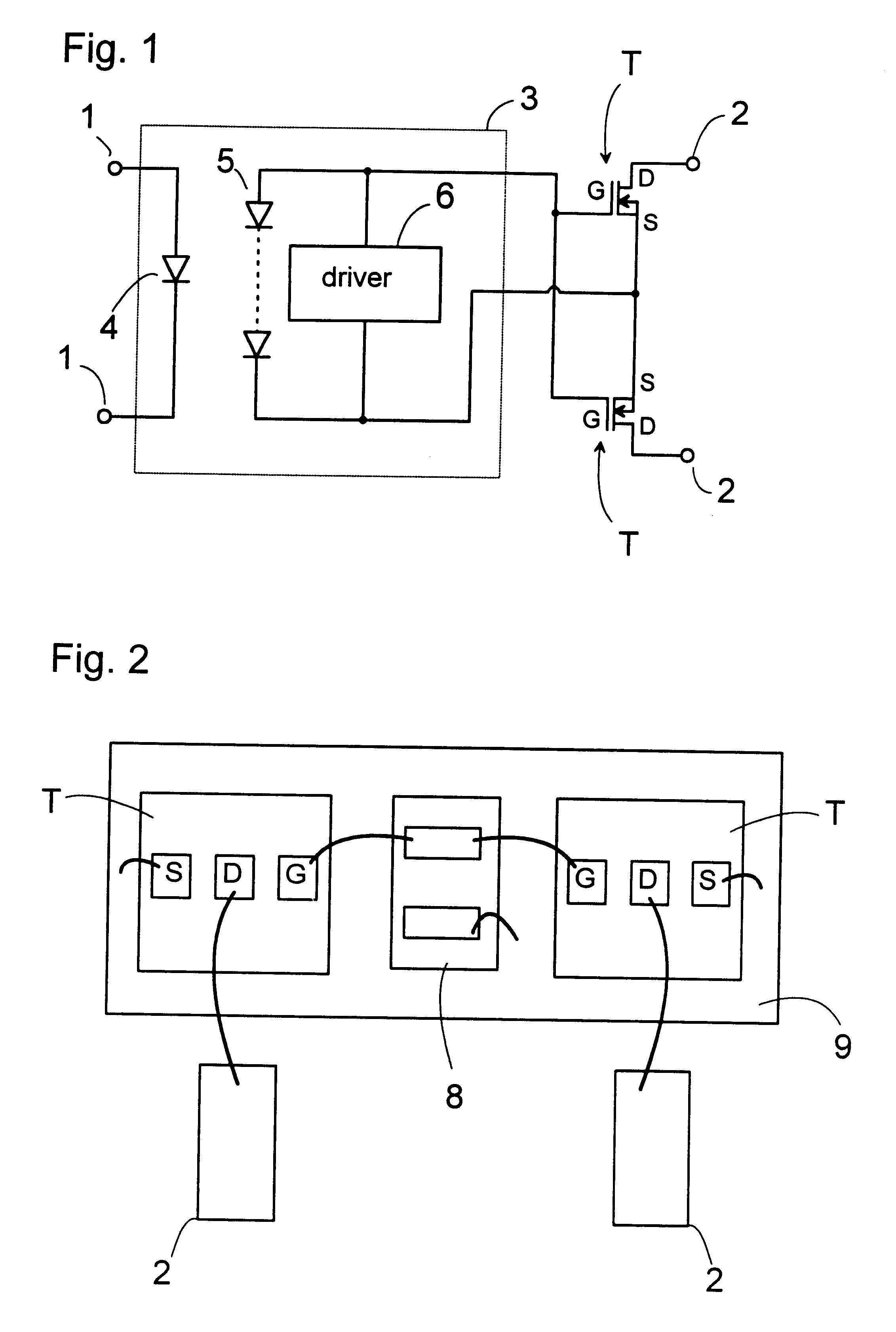
FIG. 6 illustrates a solid-state relay in accordance with the present invention in which each of two MOSFETs T is mounted on a separate supporting plate 9A of electrically conductive material and has its gate connected to a like control unit chip 8A mounted on a separate frame 7. Drain of each FET is electrically connected to each supporting plate 9A formed with an output terminals 2A as an integral part thereof.

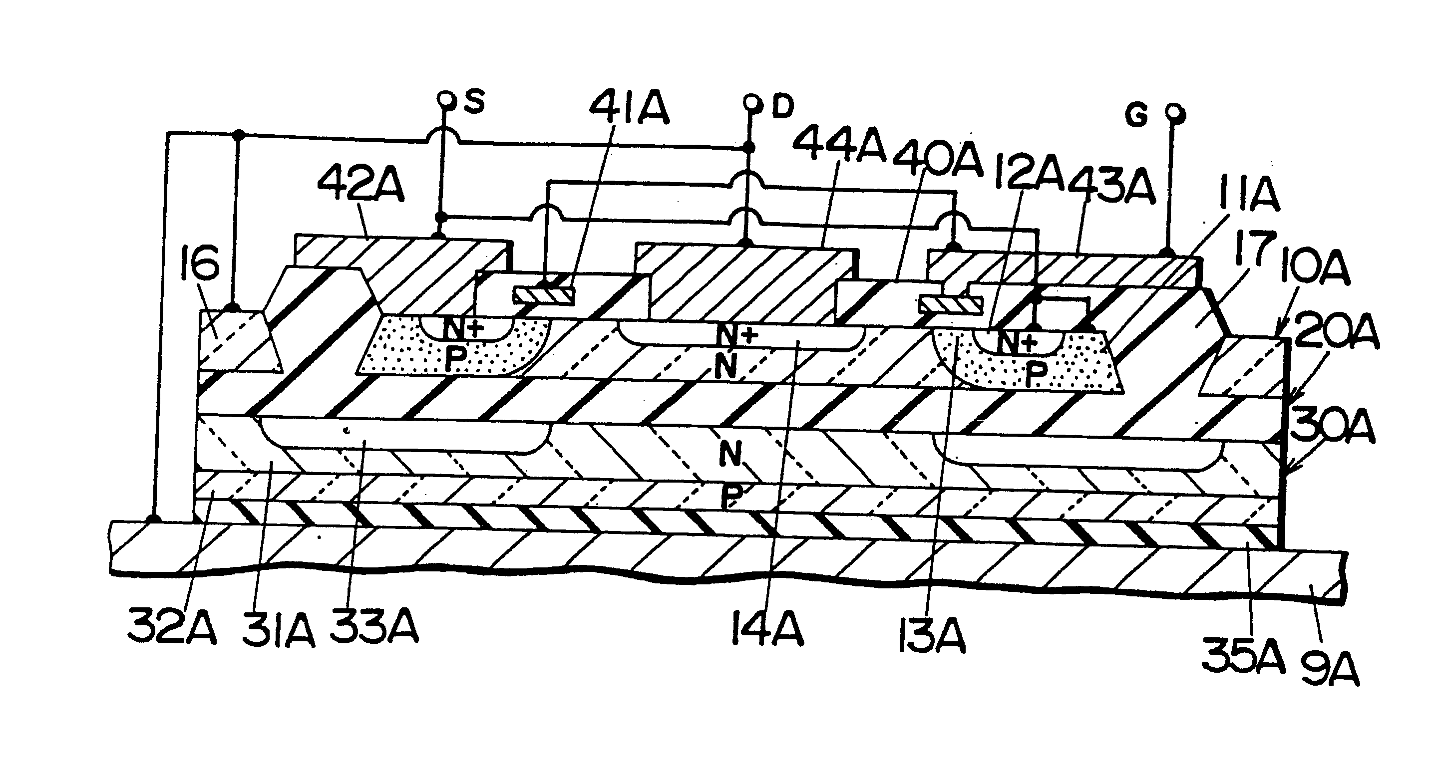
As shown in FIGS. 7 and 8, FET is also of the SOI structure having an N-type silicon layer 10A, a buried oxide layer 20A, and a silicon substrate 30A. A P-type well region 11A of a closed loop configuration is diffused in the silicon layer 10A over the full depth thereof so as to leave therearound a peripheral isolated zone 16. A P-type source region 12A of the like closed loop configuration is diffused in the top surface of the well region 11A to define the source of FET as well as to define a channel 13A between the source region 12A and a confronting inner periphery of th...

first embodiment

Also in this embodiment, the silicon substrate 30A is composed of an N-type upper stratum 31A and a P-type lower stratum 32A placed on the supporting plate 9A through a dielectric layer 35A. The upper stratum 31A includes a cavity 33A of annular configuration in a horizontal plane which is formed at an interface with the buried oxide layer 20A to extend horizontally in an opposed relation to a portion of the silicon layer 10A covering the well region 11A and the separator ring 17. The cavity 33A, the P-N interface between the stratums 31A and 32A, as well as the dielectric layer 35A function to reduce the overall drain-source capacitance in the same manner as explained with reference to the

third embodiment

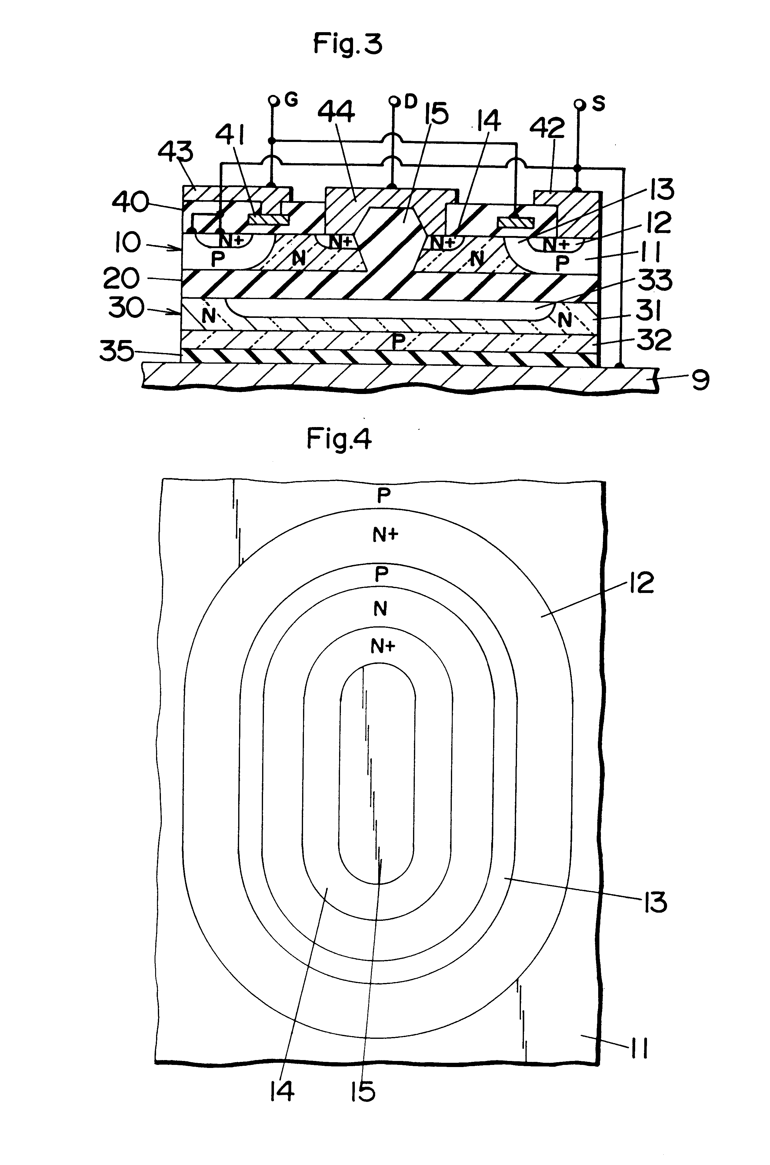
FIGS. 10 to 12 illustrate another structure of SOI-LDMOSFET in accordance with the present invention. FET of illustrated structure is adapted in use for the circuit configuration as shown in FIG. 6, and comprises a N-type silicon layer 10B, buried oxide layer 20B, and a silicon substrate 30B. A P-type well region 11B of a closed loop configuration is diffused in the silicon layer 10B over the full depth thereof so as to leave therearound a peripheral isolated zone 16B. A P-type source region 12B of the like closed loop is diffused in the top surface of the well region 11B to define a channel 13B between the source region 12B and a confronting inner periphery of the well region 11B. An N-type drain region 14B is diffused centrally in the top surface of the silicon layer 10B within a confine of the well region 11B. Locally diffused in the peripheral zone 16B are a pair of P-type land 18 which extend the full depth of the silicon layer 10B and arranged in a horizontal plate to be diame...


PUM


Abstract

A solid state relay composed of a series connected pair of LDMOSFETs has a minimized output capacitance. Each LDMOSFET is configured to have a silicon layer of a first conductive type, a drain region of the first conductive type diffused in the top surface of the silicon layer, a well region of a second conductive type diffused in the silicon layer in a laterally spaced relation from the drain region, and a source region of the first conductive type diffused within the well region to define a channel extending between the source region and a confronting edge of the well region along the top surface of the silicon layer. Each LDMOSFET is of an SOI (Silicon-On-Insulator) structure composed of a silicon substrate placed on a supporting plate, a buried oxide layer on the silicon substrate, and the silicon layer on the buried oxide layer. The well region is diffused over the full depth of the silicon layer to have its bottom in contact with the buried oxide layer, so that the well region forms with the silicon layer a P-N interface only at a small area adjacent the channel. Because of this reduced P-N interface and also because of the buried oxide layer exhibiting a much lower inductive capacitance than the silicon layer, it is possible to greatly reduce a drain-source capacitance for minimizing the output capacitance of the relay in the non-conductive condition.

Description

1. Field of the InventionThe present invention is directed to a solid-state relay, and more particularly to a solid-state relay having a pair of LDMOSFETs of which drains define output terminals for connection with a load to be controlled by the relay.2. Description of the Prior ArtSolid-state relays have been widely utilized in place of mechanical relays in view of many advantages including miniaturized configuration, low-energy consumption, and high-speed switching performance. Because of the above advantages, the solid-state relay can be successfully incorporated in a small device, such as an automatic test equipment for testing LSI chips, for example. When utilized for the measurement of this kind, the relay is designed to provide a series of output signal as a testing signal. As the frequency of the output signal becomes higher, the relay is required to have a lower output capacitance developed across output terminals of the relay during off-periods of the output signal, i.e., ...

Claims


Application Information

Patent Timeline
Patent Type & Authority Patents(United States)
IPC IPC(8): H01L29/78H01L23/48H01L29/02H01L29/06H01L29/66H01L23/495H01L27/12H01L27/085H01L27/088
CPCH01L23/49562H01L23/49575H01L24/06H01L24/49H01L27/088H01L27/1203H01L29/0649H01L29/0653H01L29/0696H01L29/7824H01L2924/1306H01L2224/05554H01L2224/05553H01L2224/32245H01L24/48H01L2924/12041H01L2924/30105H01L2924/19043H01L2924/14H01L2924/13091H01L2924/01082H01L2224/05624H01L2224/48091H01L2224/48137H01L2224/48237H01L2224/48257H01L2224/49H01L2224/73265H01L2924/01013H01L2924/01014H01L2924/01015H01L2924/01033H01L2924/00014H01L2924/00H01L2924/12036H01L2224/45099H01L27/12
Inventor SUZUMURA, MASAHIKOTAKANO, HITOMICHISUZUKI, YUJIKISHIDA, TAKASHIHAYASAKI, YOSHIKISHIRAI, YOSHIFUMIYOSHIDA, TAKESHIMIYAMOTO, YASUNORI
Owner MATSUSHITA ELECTRIC WORKS LTD
Why Eureka
Try Eureka