Convertible hot edge ring to improve low-K dielectric etch

a dielectric etch and hot edge technology, applied in the manufacture of semiconductor/solid-state devices, basic electric elements, electric apparatus, etc., can solve the problems of slow operation of semiconductor devices, insufficient conductive line isolation, and sio dielectric layers formed in layers 2

Inactive Publication Date: 2002-05-07
LAM RES CORP
View PDF23 Cites 78 Cited by
  • Summary
  • Abstract
  • Description
  • Claims
  • Application Information

AI Technical Summary

Problems solved by technology

This introduces an increased level of coupling capacitance to the circuit, which has the drawback of slowing the operation of the semiconductor device.
As a consequence of the increasing line densities and operating frequencies in semiconductor devices, dielectric layers formed of SiO.sub.2 may not effectively insulate the conductive lines to the extent required to avoid increased coupling capacitance levels.
Although chemistries that use fluorocarbons as passivants give reasonable etch rates and profile control, the free fluorine from the fluorocarbon causes poor selectivity to the oxide hardmask.
This particularly affects corner selectivity where the oxide hardmask is first exposed, and as a result CDs are degraded.
The hard mask layer is employed since photoresist is typically ineffective as a masking material when etching the organic low-K material of low capacitance dielectric layer 106.
This bowing effect degrades profile control, for example, causing the formation of re-entrant profiles, which are profiles that have angles greater than 90 degrees, and cause difficulties in subsequent processing steps such as metal fill.
With this enlargement, the critical dimension of the via / trench may be lost.
If too little fluorocarbon is added, there may be insufficient passivation to maintain the desired vertical sidewall profile.
Even where appropriate etchant / diluent / passivant combinations are employed, uniformity of the etch process across the surface of the wafer is often a problem.

Method used


Image

  • Convertible hot edge ring to improve low-K dielectric etch
  • Convertible hot edge ring to improve low-K dielectric etch
  • Convertible hot edge ring to improve low-K dielectric etch

Examples


Embodiment Construction

and in conjunction with the following figures.

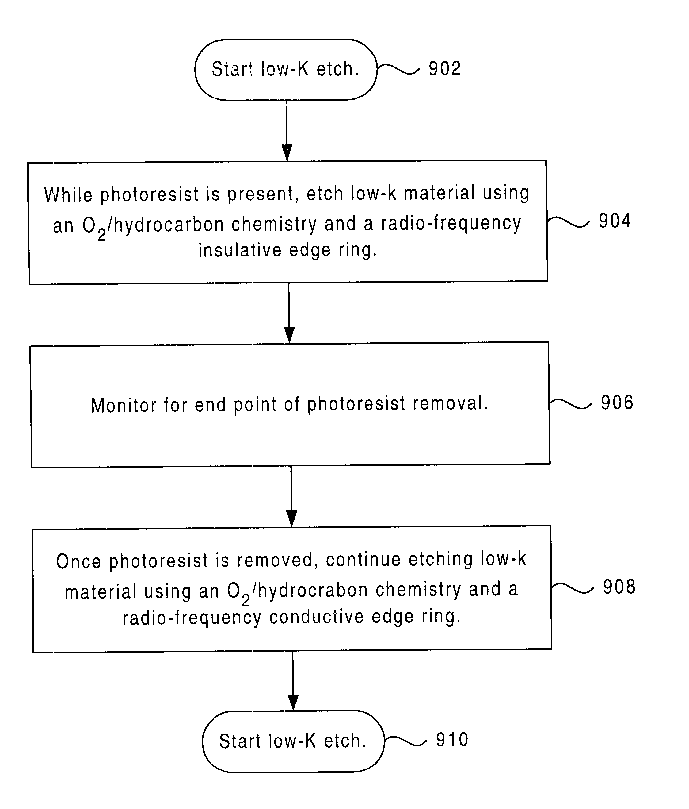
The present invention teaches a two-step process to improve low-K dielectric etch uniformity on a wafer bearing a low-K layer, a hard mask layer, and a photoresist layer. The etching process takes place in a reactor vessel. According to a first aspect of the present invention, in a first etching step while photoresist is present the low-K material is etched using a first etchant including an oxygen-bearing compound and a hydrocarbon passivant in the presence of a radio-frequency insulative edge ring. When the photoresist is determined to be substantially cleared from the wafer, for instance by means of a clearing signal generated by detectors and end-point software, a second etching step is performed. In the second etching step, the low-K material is etched using a second etchant including an oxygen-bearing compound and a hydrocarbon passivant in the presence of a radio-frequency conductive edge ring. Hydrocarbons may, in accordance with...


PUM


Abstract

Two-step process to improve low-K dielectric etch uniformity, apparatus to perform the method, and semiconductor devices formed in accordance with the method. In a first etching step, an insulating hot edge ring is provided. When the photoresist clearing signal is observed using end-point software, the insulating cover is moved aside to expose the conductive edge ring for the remainder of the etch. One aspect of this invention contemplates an insulator cover over a conductive edge ring at the start of wafer etching, which cover is removed after end-pint detection. The present invention contemplates a number of physical configurations whereby the insulator ring is urged into, and away from, its masking of the conductive edge ring. Alternatively, the etching of a wafer bearing low-K material may be conducted using two edge rings, where the first etch step is conducted using an insulating hot edge ring, and a second etch step is conducted using a conductive hot edge ring. According to this aspect, the two step process may thus be performed in a plurality of reactor vessels, or in one reactor vessel having a plurality of processing stations. Different low-K materials may require differing etchant / passivant / diluent combinations. Accordingly, the two-step etch process is taught in conjunction with any number of different etch chemistries.

Description

1. Field of the InventionThe present invention relates to the manufacture of semiconductor devices. More particularly, the present invention teaches a novel method for etching semiconductor devices incorporating low dielectric constant organic films, such as SiLK.RTM., while maintaining one or more desirable feature attributes, including feature critical dimension.2. Description of Related ArtIntegrated circuits use dielectric layers, which have typically been formed from silicon dioxide, SiO.sub.2, to insulate conductive lines on various layers of a semiconductor structure. As semiconductor circuits become faster and more compact, operating frequencies increase and the distances between the conductive lines within the semiconductor device decrease. This introduces an increased level of coupling capacitance to the circuit, which has the drawback of slowing the operation of the semiconductor device. Therefore, it has become important to use dielectric layers that are capable of effec...

Claims


Application Information

Patent Timeline
Patent Type & Authority Patents(United States)
IPC IPC(8): H01L21/00H01L21/02H01L21/311
CPCH01L21/67069H01L21/31138
Inventor FLANNER, JANET M.ELLINGBOE, SUSANJANOWIAK, CHRISTINELANG, JOHNMOREY, IAN J.
Owner LAM RES CORP
Why Eureka
Try Eureka