Optical semiconductor device with resonant cavity tunable in wavelength, application to modulation of light intensity

a technology of optical semiconductors and resonant cavities, applied in the field of optical semiconductor devices with resonant cavity tunable, can solve the problems of difficult manufacturing and consequently high cost, use of deformable membranes gives a fairly long response time, and the type of diodes has a very long response tim

Inactive Publication Date: 2002-05-28
XANTIMA
View PDF9 Cites 43 Cited by
  • Summary
  • Abstract
  • Description
  • Claims
  • Application Information

AI Technical Summary

Problems solved by technology

However, it is difficult to make and consequently is fairly expensive.
Furthermore, the use of a deformable membrane gives a fairly long response time, of the order of 1 .mu.s.
This type of diode has a very long response time, of the order of 1 second, and a fairly limited tunability range.
The response time of this type of diode is of the order of 1 millisecond and they are also large and very expensive.
However, these diodes are difficult to make and therefore expensive and also require complex electronic means to control the laser radiation wavelength since three electrical currents are necessary for this purpose (one current for each of the regions mentioned above).

Method used


Image

  • Optical semiconductor device with resonant cavity tunable in wavelength, application to modulation of light intensity
  • Optical semiconductor device with resonant cavity tunable in wavelength, application to modulation of light intensity
  • Optical semiconductor device with resonant cavity tunable in wavelength, application to modulation of light intensity

Examples


Embodiment Construction

We will now compare the invention with known devices described in document [2].

A vertical emission device of the VCSEL or LED type according to the invention is distinguished from known diodes described in document [2] in that its manufacturing process is much simpler and its switching speed is much higher due to its radically different operating principle.

Furthermore, this type of device according to the invention can be made using a single control current which very much simplifies the integration of this device into optoelectronic systems.

The tunability of this type of device is about 10 nm and its response time is equal to about 1 nanosecond.

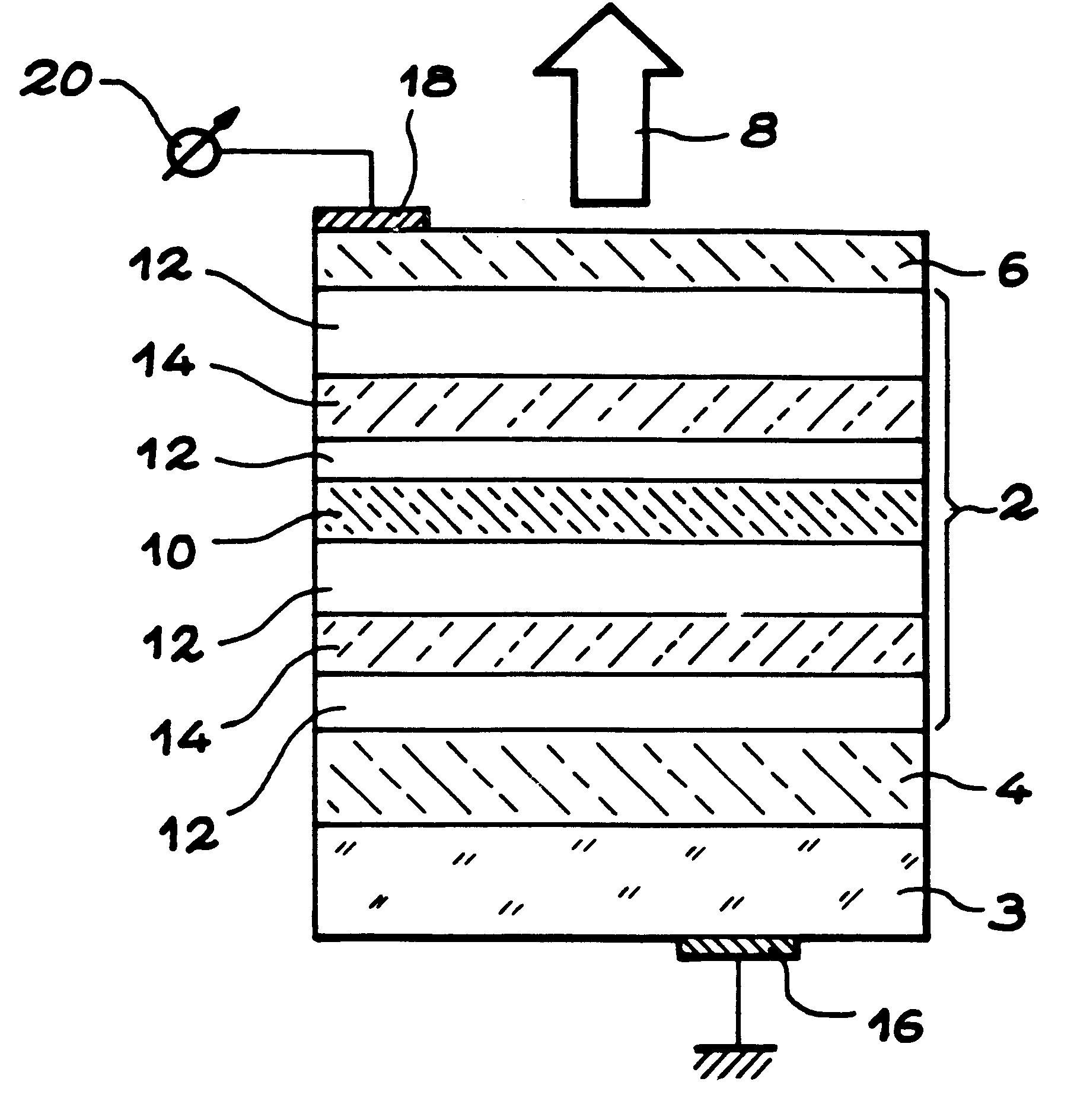
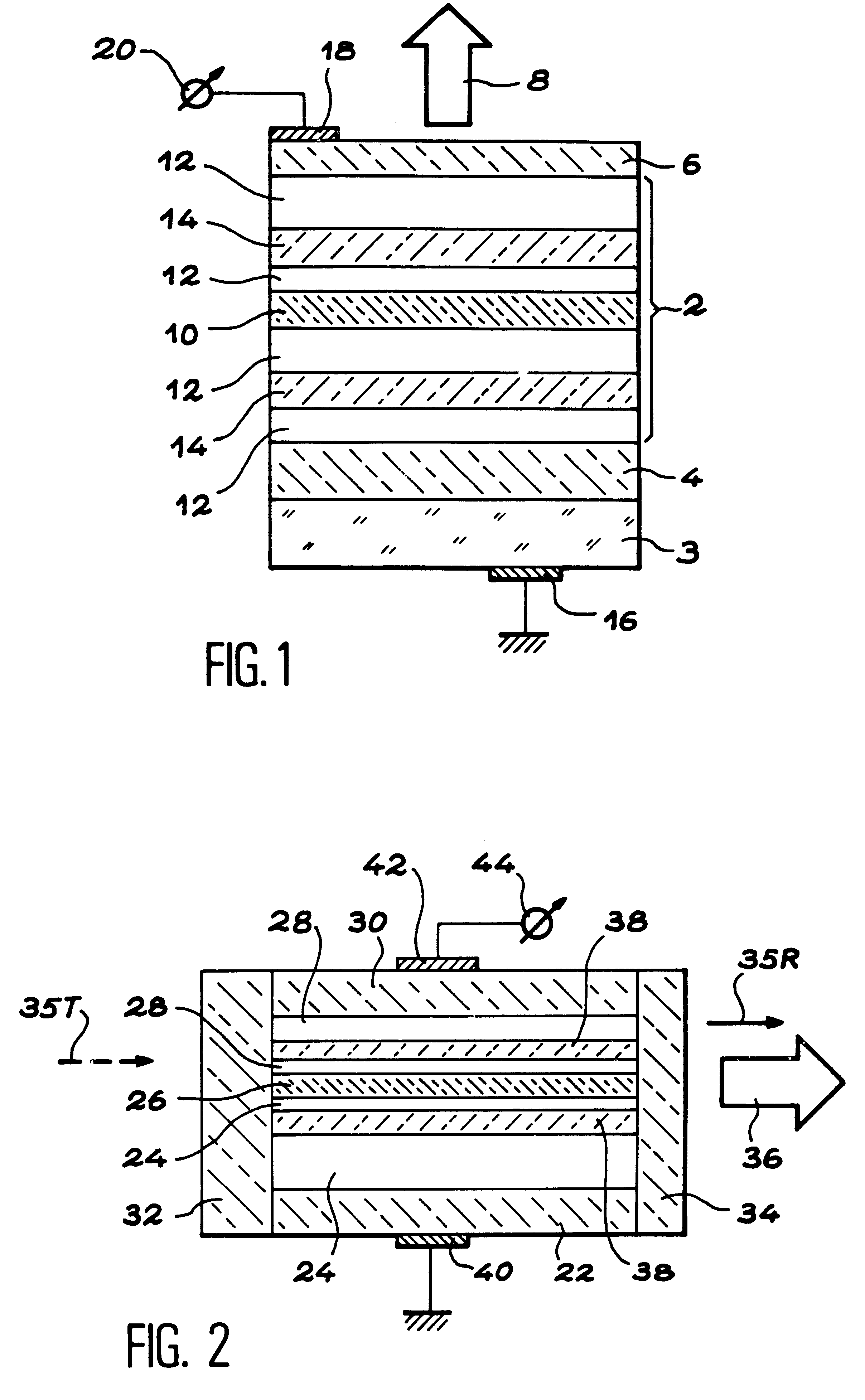
FIG. 1 diagrammatically shows a vertical emission semiconductor device emitting light according to the invention. This device comprises a resonant micro-cavity 2 formed on an N type semiconducting substrate 3 and delimited by a lower mirror 4 made of an N type semiconducting material in contact with the substrate, and an upper mirror 6 made ...


PUM

PropertyMeasurementUnit
lengthaaaaaaaaaa
response timeaaaaaaaaaa

Abstract

Optical semiconductor device with resonant cavity tunable in wavelength, application to modulation of light intensity.This device comprises a resonant cavity (2) delimited by two mirrors (4, 6) and at least one super-lattice (14) that is placed in the cavity and is formed from piezoelectric semiconducting layers, and means (20) of injecting charge carriers into the super-lattice. The optical properties of this super-lattice can thus be modified and the wavelength of cavity resonance modes can be offset. The invention is particularly applicable to optical telecommunications.

Description

This invention relates to an optical semiconductor device with resonant cavity tunable in wavelength.This device may equally well be made in the form of a coherent light source, for example a vertical emission laser also called VCSEL in the rest of this document, or an edge emission laser, or in the form of an incoherent light source, for example a light emitting diode also called LED throughout the rest of this document and with vertical emission or edge emission.The device according to the invention may also be made in the form of an optical modulator operating in reflection or in transmission.The invention is used in a variety of fields, for example such as optical telecommunications, all optical networks, information display and spectroscopy.STATE OF PRIOR ARTNote that in a vertical emission diode, the mirrors that delimit the resonant cavity of the diode are formed perpendicular to the growth axis of the layers surrounding the active area and the spacer located in the cavity. T...

Claims


Application Information

Patent Timeline
Patent Type & Authority Patents(United States)
IPC IPC(8): G02F1/017G02F1/01G02F1/21H01S5/062H01S5/183H01S5/00G02F1/015H01S5/32H01S5/34H01L33/00H01L33/06H01L33/16H01L33/28H01L33/32H01S5/10H01S5/323
CPCB82Y20/00G02F1/017G02F1/218H01S5/0622H01S5/183G02F2001/0151G02F2001/0154G02F2001/0175H01S5/3409G02F2201/346G02F2203/055H01S5/3216G02F2001/213G02F1/0154G02F1/0175G02F1/0151G02F1/213
Inventor ORTIZ, VALENTINPELEKANOS, NIKOLAOS
Owner XANTIMA
Why Eureka
Try Eureka