Low noise, low distortion RF amplifier topology

a low-noise, rf amplifier technology, applied in the field of electronic circuits and systems, can solve the problems of inherently producing high intermodulation distortion, noise and distortion introducing inaccuracies in the output signal, and no method for simultaneously minimizing both noise and distortion in an rf amplifier

Inactive Publication Date: 2002-06-04
MICROELECTRONICS TECH INC
View PDF4 Cites 3 Cited by
  • Summary
  • Abstract
  • Description
  • Claims
  • Application Information

AI Technical Summary

Problems solved by technology

Inevitably, noise and distortion introduce inaccuracies in the output signal, which will then be propagated throughout the rest of the system.
The large signal currents in the larger transistors, however,

Method used


Image

  • Low noise, low distortion RF amplifier topology
  • Low noise, low distortion RF amplifier topology
  • Low noise, low distortion RF amplifier topology

Examples


Embodiment Construction

Illustrative embodiments and exemplary applications will now be described with reference to the accompanying drawings to disclose the advantageous teachings of the present invention.

While the present invention is described herein with reference to illustrative embodiments for particular applications. it should be understood that the invention is not limited thereto. Those having ordinary skill in the art and access to the teachings provided herein will recognize additional modifications, applications, and embodiments within the scope thereof and additional fields in which the present invention would be of significant utility.

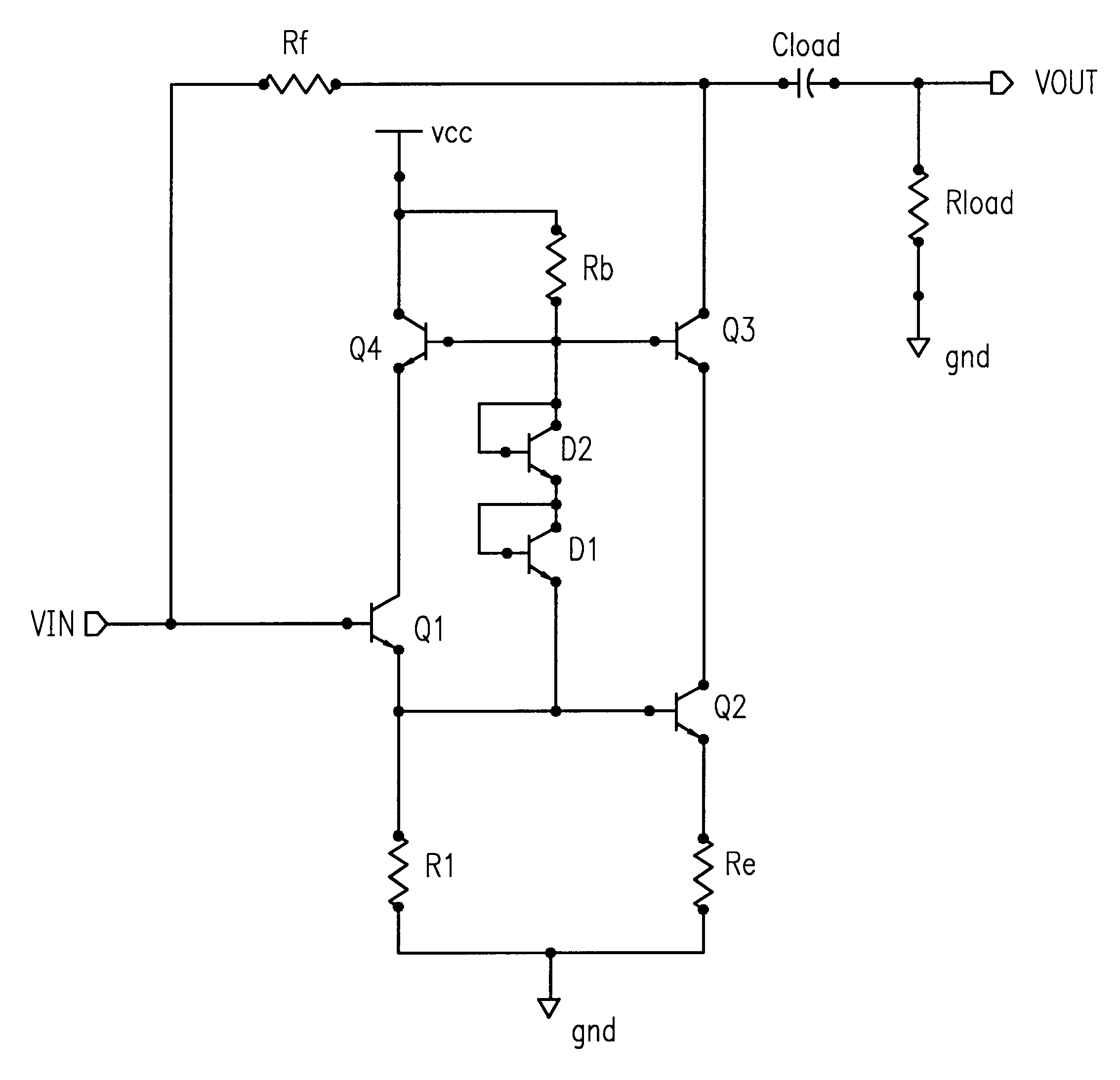
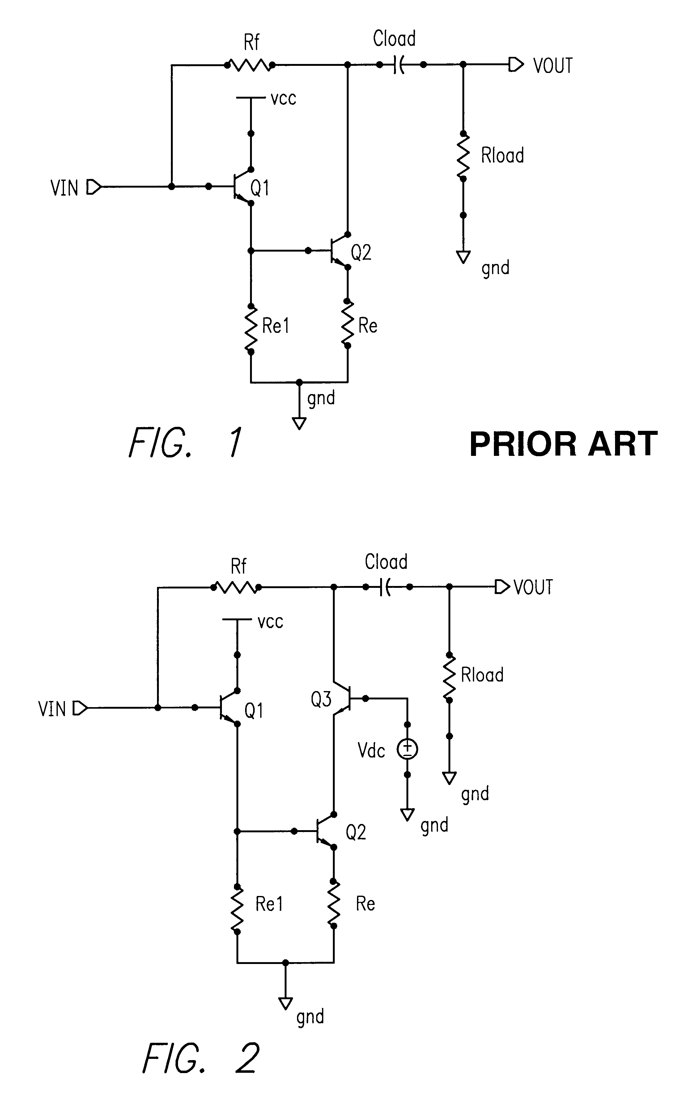
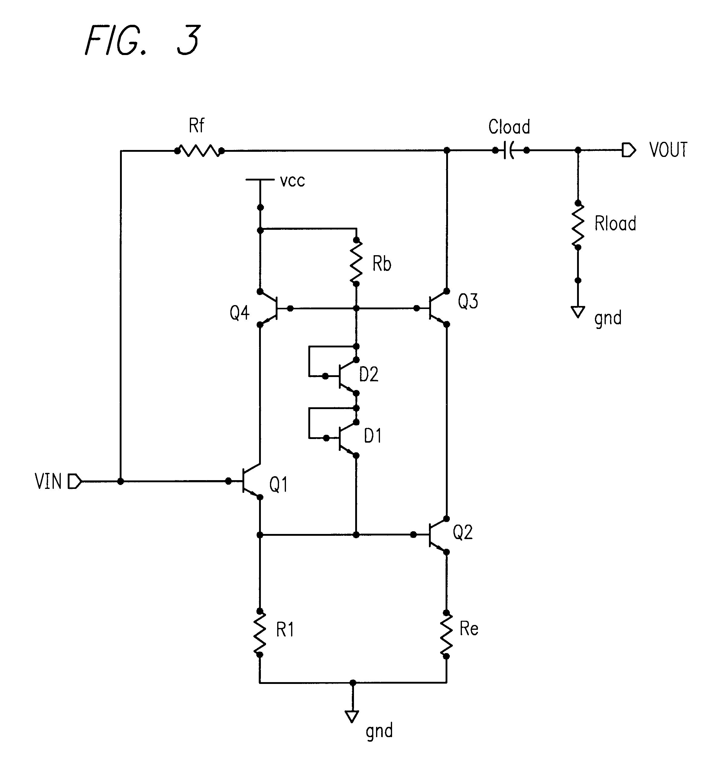
FIG. 1 is a simplified schematic diagram of a simple low noise amplifier such as that currently used in RF amplifiers of conventional design and construction. The amplifier includes first and second transistors Q1 and Q2 connected in a common collector, common emitter cascade. The first transistor Q1 is in a common collector configuration, the second transistor ...


PUM


Abstract

A low noise, low distortion radio frequency amplifier which includes a bootstrap design to minimize intermodulation distortion while simultaneously achieving low noise and wide bandwidth. In the illustrative embodiment, the invention includes a first circuit for receiving an input signal; a second circuit for amplifying the input signal using a transistor Q2; and a third circuit for regulating a rate of change of voltage across the transistor Q2 such that the rate of voltage change is zero. The third circuit includes a transistor Q3 connected to the transistor Q2 in cascode. In the specific illustrative embodiment, the third circuit further includes two diodes D1 and D2 used to modulate the voltage at the input of the transistor Q3 in proportion to the voltage modulation at the input of the transistor Q2. In the illustrative embodiment, the second circuit includes a transistor Q1 connected in cascade to the transistor Q2. In the specific illustrative embodiment, the invention further includes a fourth circuit for regulating a rate of change of voltage across the transistor Q1 such that the rate of voltage change is zero. The fourth circuit includes a transistor Q4 connected to the transistor Q1 in cascode. The two diodes D1 and D2 also connect the transistors Q1 and Q4 such that the voltage at the input of the transistor Q4 is modulated in proportion to the voltage modulation at the input of the transistor Q1.

Description

1. Field of the InventionThe present invention relates to electronic circuits and systems. More specifically, the present invention relates to radio frequency amplifiers used in communications systems.2. Description of the Related ArtSignal integrity is a critical consideration in the design and operation of amplifier circuits, particularly when used in transmitters and receivers for communications systems. For a variety of applications, it is imperative that the output of the amplifier accurately tracks the input. Inevitably, noise and distortion introduce inaccuracies in the output signal, which will then be propagated throughout the rest of the system. In this connection, the term `noise` refers to the thermal noise generated by the circuit, while `distortion` refers to the nonlinearities produced by the circuit design such as harmonics or intermodulation products.Currently, conventional low noise amplifiers are designed to keep the thermal noise level to a minimum by using large...

Claims


Application Information

Patent Timeline
IPC IPC(8): H03F1/08H03F3/42H03F1/34H03F1/22
CPCH03F1/22H03F3/42H03F1/34H03F2200/372
Inventor TRAN, KELVIN T.DUONG, CLIFFORDFARIAS, MICHAEL N.DEVENDORF, DON C.LINDER, LLOYD F.
Owner MICROELECTRONICS TECH INC
Why Eureka
Try Eureka