Isolation region forming methods
- Summary
- Abstract
- Description
- Claims
- Application Information
AI Technical Summary
Problems solved by technology
Method used
Image
Examples
first embodiment
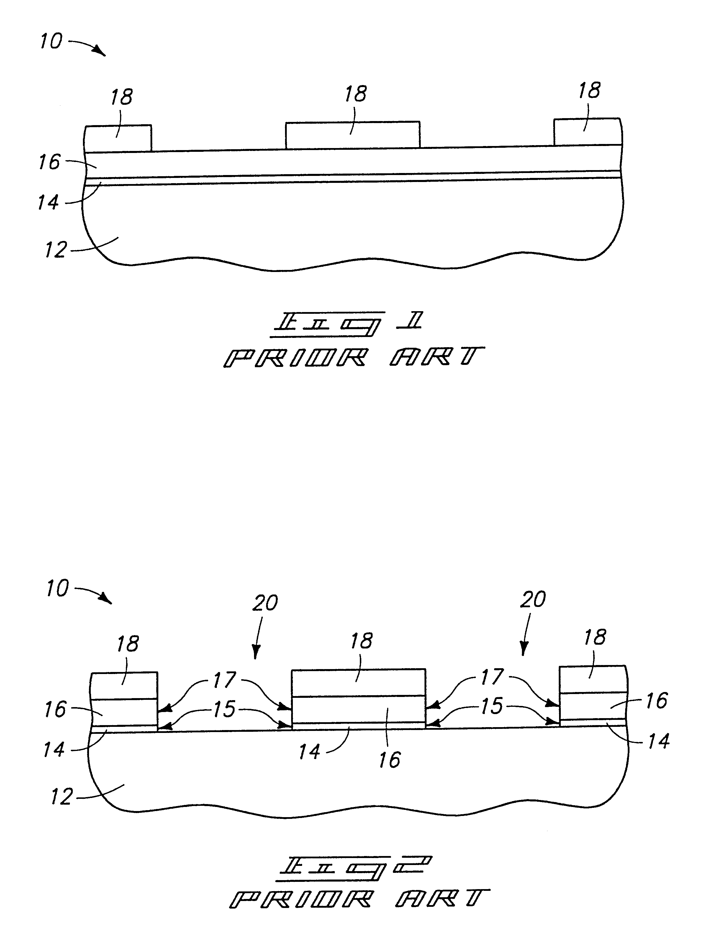
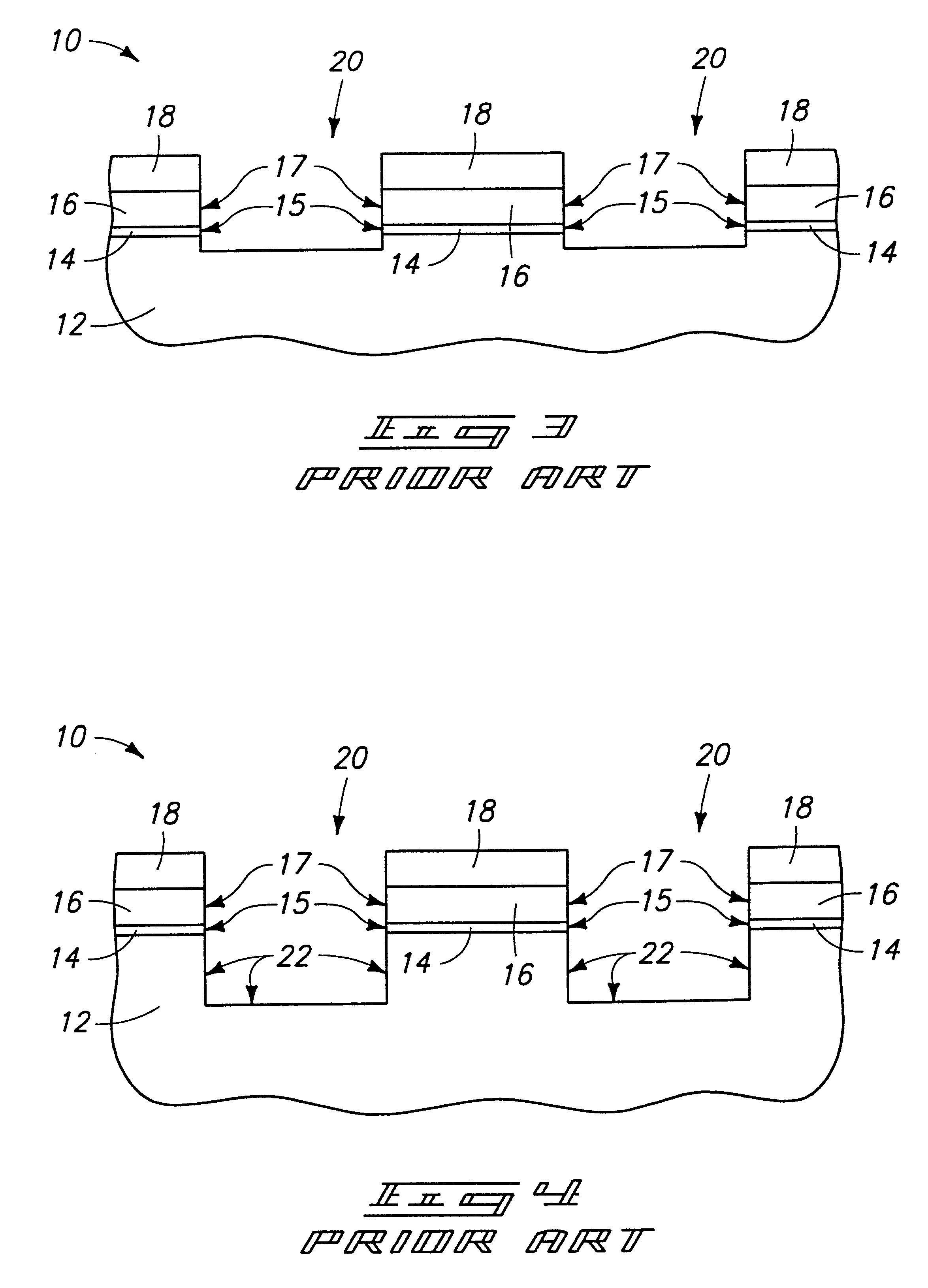
FIG. 13 illustrates a semiconductor wafer fragment 10a at a preliminary stage of the first embodiment method. Specifically, wafer fragment 10a is illustrated at a processing step subsequent to the prior art step of FIG. 3. Wafer fragment 10a comprises a semiconductive substrate 12, an oxide layer 14, a nitride layer 16, and a photoresist layer 18. Openings 40 extend through oxide layer 14 and nitride layer 16 and into substrate 12. Oxide layer 14 and nitride layer 16 ultimately function as masking layers during formation of an isolation region, and so can be referred to as a first masking layer 14 and a second masking layer 16.
The formation of openings 40 can be initiated by processing identical to that described above with reference to prior art FIG. 3. Specifically, openings 20 (FIG. 3) are formed by transferring a pattern from photoresist layer 18 through first and second masking layers 14 and 16. Openings 20 (FIG. 3) are then extended into openings 40 by etching photoresist laye...
second embodiment
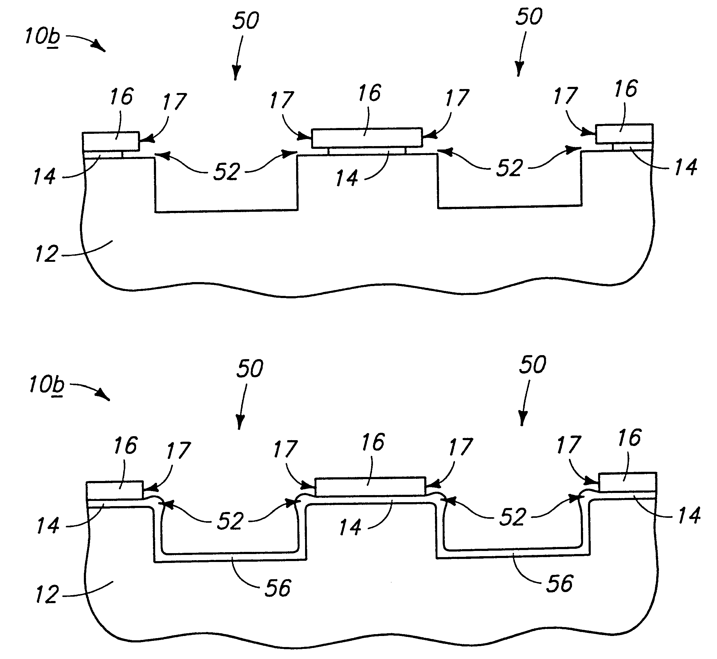
A second embodiment method of the present invention is described with reference to FIGS. 17-21. In describing the second embodiment, similar numbering to that utilized in describing the prior art of FIGS. 1-12 will be used, with differences indicated by the suffix "b" or by different numerals.
Referring to FIG. 17, a wafer fragment 10b is illustrated at a preliminary processing step of the second embodiment method. Specifically, wafer fragment 10b is illustrated at a processing step subsequent to the prior art step illustrated in FIG. 4, with photoresist layer 18 (FIG. 4) having been removed. Wafer fragment 10b comprises silicon substrate 12, oxide layer 14, and nitride layer 16, with layers 14 and 16 alternatively being referred to as first and second masking layers, respectively. Openings 50 extend through nitride layer 16 and oxide layer 14, and into substrate 12. Openings 50 can be formed in accordance with the methods described above with reference to FIG. 4 for forming openings...
third embodiment
the invention is described with reference to FIGS. 22-25. In describing the third embodiment, similar numbering to that utilized above in describing the first two embodiments will be used, with differences indicated by the suffix "c" or by different numerals.
Referring to FIG. 22, a wafer fragment 10c is shown at a preliminary stage of the third embodiment processing. Wafer fragment 10c is shown at a processing step subsequent to that of FIG. 4, with a photoresist layer 18 (FIG. 4) having been removed. Wafer fragment 10c comprises a semiconductor substrate 12, a pad oxide layer 14, and a silicon nitride layer 16, with layers 14 and 16 alternatively being referred to as first and second masking layers, respectively. Openings 60 extend through layers 16 and 14, and into substrate 12.
Referring to FIG. 23, nitride layer 16 is subjected to a facet etch to reduce a thickness of portions of nitride layer 16 proximate edges 17. The facet etching can comprise, for example, a plasma etch utili...
PUM
 Abstract
Description
Claims
Application Information
 - R&D Engineer
- R&D Manager
- IP Professional
- Industry Leading Data Capabilities
- Powerful AI technology
- Patent DNA Extraction
Browse by: Latest US Patents, China's latest patents, Technical Efficacy Thesaurus, Application Domain, Technology Topic, Popular Technical Reports.
© 2024 PatSnap. All rights reserved.Legal|Privacy policy|Modern Slavery Act Transparency Statement|Sitemap|About US| Contact US: help@patsnap.com


