Power supply unit for sputtering device

a technology of power supply unit and sputtering device, which is applied in the direction of electrolysis components, vacuum evaporation coatings, coatings, etc., can solve the problems of high probability of continuous arc discharge, damage to the substrate, and inability to effect such sputtering

Inactive Publication Date: 2002-07-09
SHIBAURA MECHATRONICS CORP
View PDF18 Cites 59 Cited by
  • Summary
  • Abstract
  • Description
  • Claims
  • Application Information

AI Technical Summary

Benefits of technology

The present invention is achieved with the above-mentioned points in view and its object is to provide a power supply device for a sputtering apparatus which, in order to prevent the generation of a continuous arc discharge, sets a time interval of the application of a reverse voltage pulse to be within 1 to 10 .mu.s in the case where the generation of the arc discharge is detected and can positively prevent the generation of a reverse arc discharge resulting from the reverse voltage pulse.

Problems solved by technology

If, in this case, the magnetron discharge is changed to the arc discharge, it is not possible to effect such sputtering.
Incidentally, the time interval in which the reverse voltage pulse was applied was required to have a time interval of a given value because a problem arises such as to protect a switching element from being destroyed due to a power loss involved.
There was a problem with a high probability of the occurrence of a continuous arc discharge.
When a continuous arc discharge has been produced due to a reverse arc discharge, there was a problem of causing damage to the substrate.

Method used


Image

  • Power supply unit for sputtering device
  • Power supply unit for sputtering device
  • Power supply unit for sputtering device

Examples


first embodiment

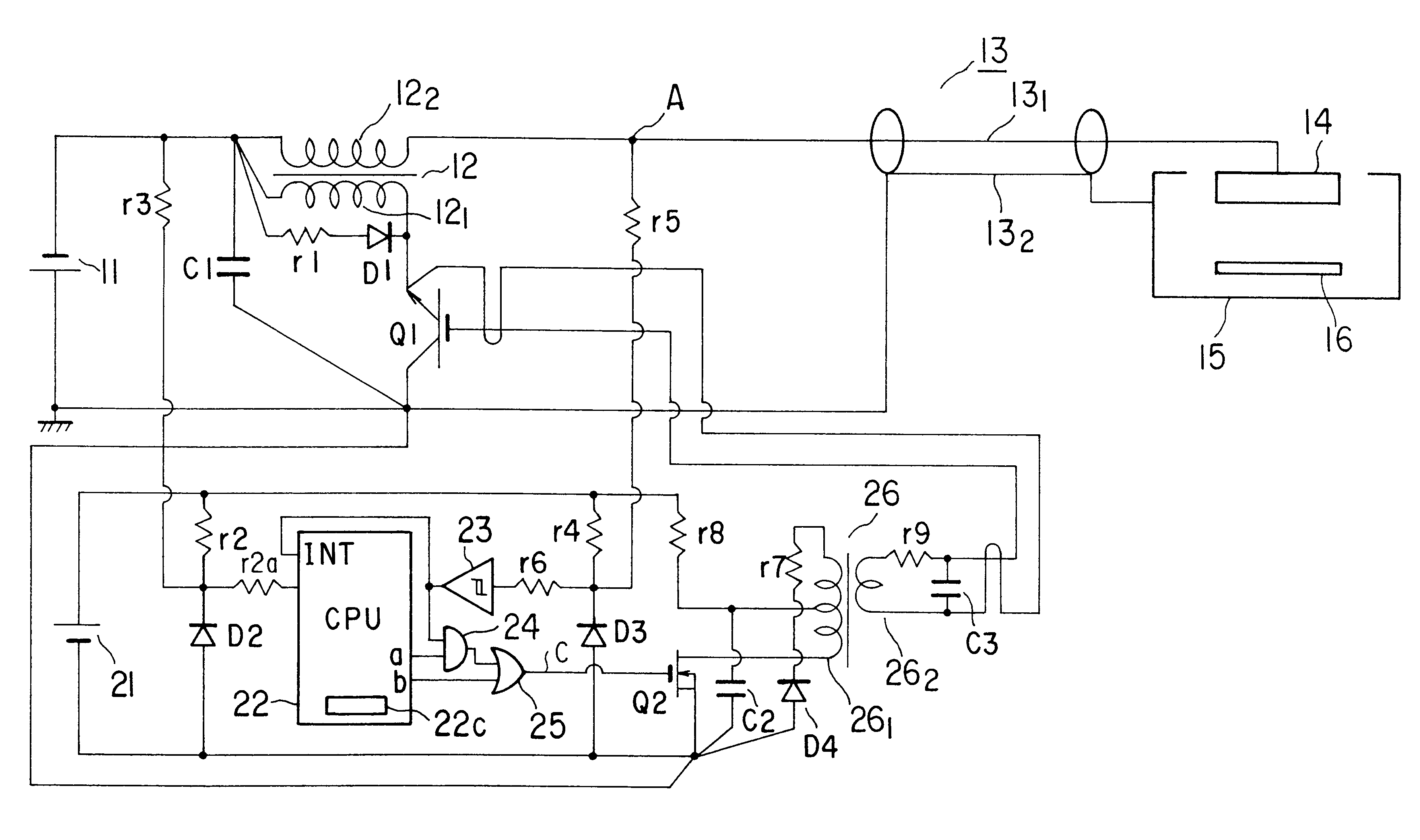
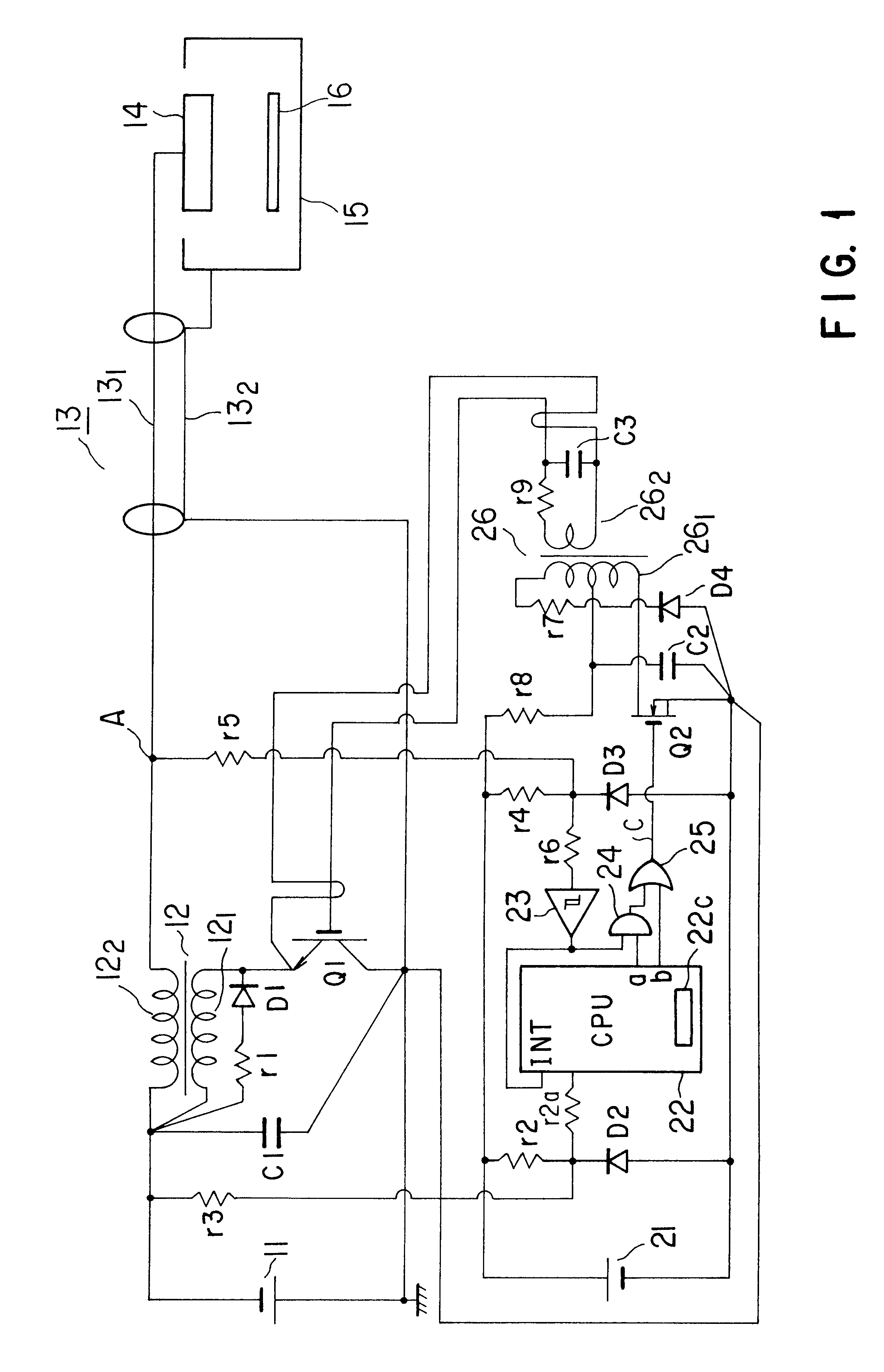
the present invention will be explained below with reference to the accompanying drawing. FIG. 1 is a circuit diagram showing a power supply device for a sputtering apparatus. In this Figure, 11 shows a DC power supply for a sputtering apparatus which is, for example, 800V. The negative electrode of the DC power supply 11 is connected to one input terminal sides of a primary coil 12.sub.1 and secondary coil 12.sub.2 in a pulse transformer 12 serving as a reverse voltage generating means. The turn ratio of the primary coil 12.sub.1 and secondary coil 12.sub.2 is set to be 1:1.1: to 1:1.3.

The other end of the primary coil 12.sub.1 is connected to the emitter of a transistor Q1 serving as a switching means. The collector of the transistor Q1 is connected to a positive electrode 11 of the DC power supply 11.

Further, a series connected circuit of a resistor r1 and diode D1 is connected in parallel between both terminals of the primary coil 12.sub.1. The resistor r1 is used for surge abso...

second embodiment

With reference to FIG. 3 an explanation will be given below about the present invention.

In the second embodiment, the same reference numerals are employed to designate parts corresponding to those shown in the first embodiment and any further explanation of them is, therefore, omitted.

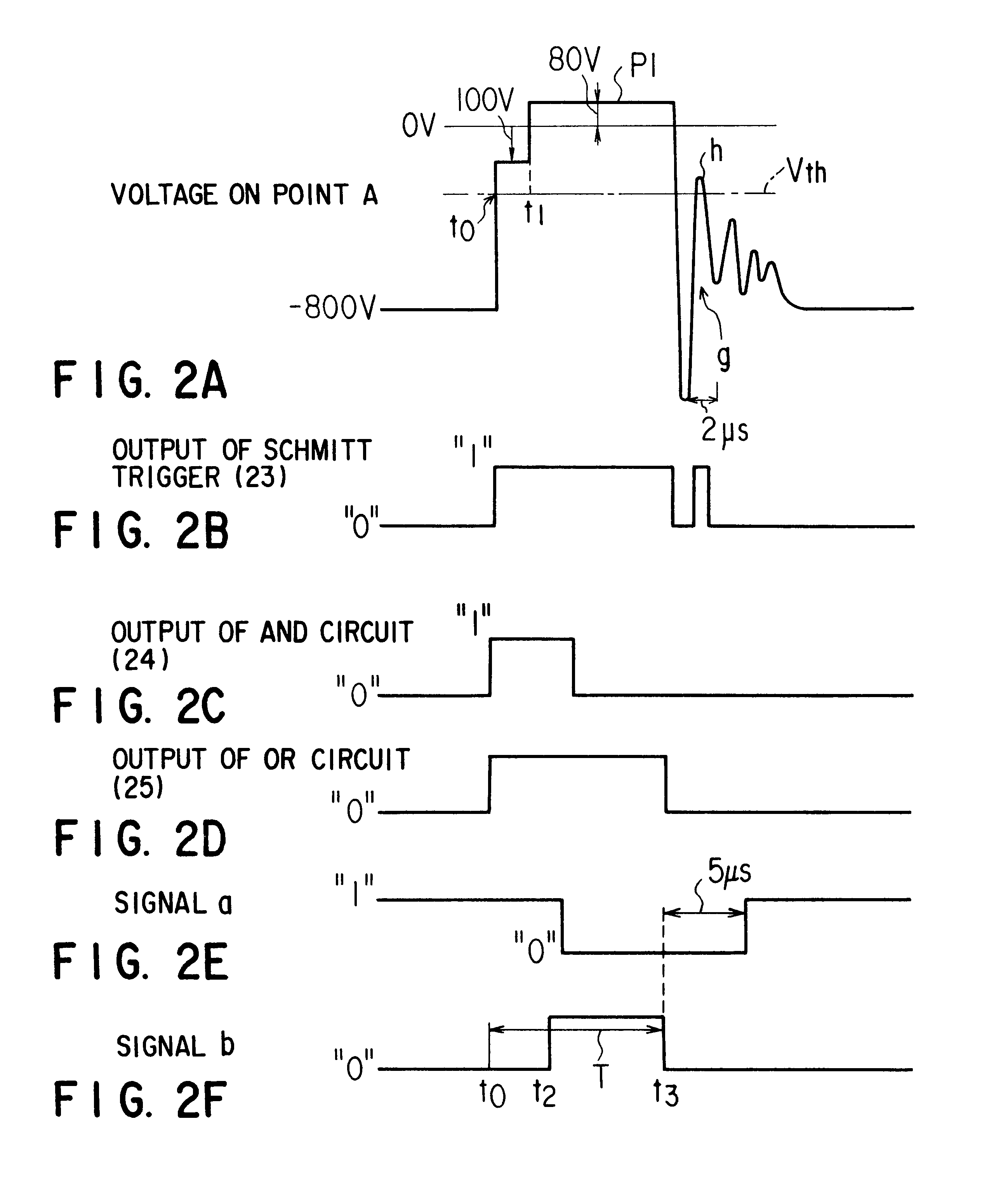
In the second embodiment, between a point A of the first embodiment in FIG. 1 and the end of one line 13.sub.1 of an output cable 13, a diode D10 is connected in a way to have its anode connected to a line 13.sub.1 side and its cathode connected to a DC power supply 11 side. And a resistor r10 is bypassed to the diode D10 and connected in parallel to the diode D10. The remaining portion of the circuit is similar to that of the first embodiment. Further, the resistor r10 is about 100 [.OMEGA.] for example as will be set out below.

By connecting the diode D10 and resistor r10 as the parallel circuit a magnetron discharge is generated in a vacuum container 15 and sputtering is carried out. In this case, a ...


PUM

PropertyMeasurementUnit
timeaaaaaaaaaa
timeaaaaaaaaaa
voltageaaaaaaaaaa

Abstract

The present invention is such that, in a circuit for preventing an arc discharge through the application of a reverse voltage pulse, in the case where, after the application of the reverse voltage pulse has been ended, the generation of an arc discharge is detected by an arc discharge detecting means (23), a reverse voltage generated by a reverse voltage generating means (12) is applied within 1 to 10 mus to a sputtering source to lower the probability of generating a continuous arc discharge and, through a diode (D10) connected in series with the sputtering source (14) and a resistor (r10) connected in parallel with the diode (D10), a current at a time of applying the reverse voltage is restricted, thus lowering a continuous arc discharge resulting from the reverse arc discharge.

Description

The present invention relates to a power supply device for a sputtering apparatus for forming a thin film on an electronic component, semiconductor, optical disk, etc.The technique for forming a thin film on a semiconductor, electronic component, decorated component, etc., by means of a sputtering apparatus using a sputtering source arranged with a magnet placed at a rear surface of a target has been extensively used. In such a sputtering apparatus, an inert gas, such as Ar, is introduced as a discharge gas in a vacuum chamber with a sputtering source placed therein and, by applying a negative voltage to the sputtering source, a magnetron discharge is generated, causing the ionization of the discharge gas introduced in the vacuum container, the acceleration of positive ions of ionized argon and the subsequent collision of these against the target surface of the sputtering source, so that the target surface is evaporated through the sputtering. The sputtering particles are deposited ...

Claims


Application Information

Patent Timeline
Patent Type & Authority Patents(United States)
IPC IPC(8): C23C14/54H01J37/32H01J37/34C23C14/34
CPCC23C14/54H01J37/34H01J37/3444H01J2237/0206C23C14/34
Inventor KURIYAMA, NOBORUYATSU, YUTAKAKAWAMATA, YOSHIOFUJII, TAKASHI
Owner SHIBAURA MECHATRONICS CORP
Why Eureka
Try Eureka