Silicon-on-insulator (SOI) substrate, method for fabricating SOI substrate and SOI MOSFET using the SOI substrate

a technology of silicon-on-insulator and substrate, applied in the field of silicon-on-insulator (soi) substrate, can solve the problems of low integration of semiconductor devices, dynamic leakage, and large siz

Inactive Publication Date: 2002-08-20
SAMSUNG ELECTRONICS CO LTD
View PDF8 Cites 71 Cited by
  • Summary
  • Abstract
  • Description
  • Claims
  • Application Information

AI Technical Summary

Problems solved by technology

However, the wide isolation region results in larger size and low integration of a semiconductor device.
However, the floating body regions 15, 17 may cause fluctuations in voltage, which leads to many problems such as a kink effect, low breakdown voltage of a drain due to a parasitic horizontal bi-polar transistor, dynamic leakage of current and an output characteristic of history dependence and instability in the SOI CMOS transistor.
Unfortunately, it is quite difficult to make an effective body contact in the SOI CMOS transistor, and a H type body contact is the most frequently used one at present.
Thus, it is difficult to effectively set the u

Method used


Image

  • Silicon-on-insulator (SOI) substrate, method for fabricating SOI substrate and SOI MOSFET using the SOI substrate
  • Silicon-on-insulator (SOI) substrate, method for fabricating SOI substrate and SOI MOSFET using the SOI substrate
  • Silicon-on-insulator (SOI) substrate, method for fabricating SOI substrate and SOI MOSFET using the SOI substrate

Examples


Embodiment Construction

Preferred embodiments of the SOI substrate, the method for fabricating the SOI substrate and the SOI MOSFET of the invention will now be described in detail with reference to the accompanying drawings.

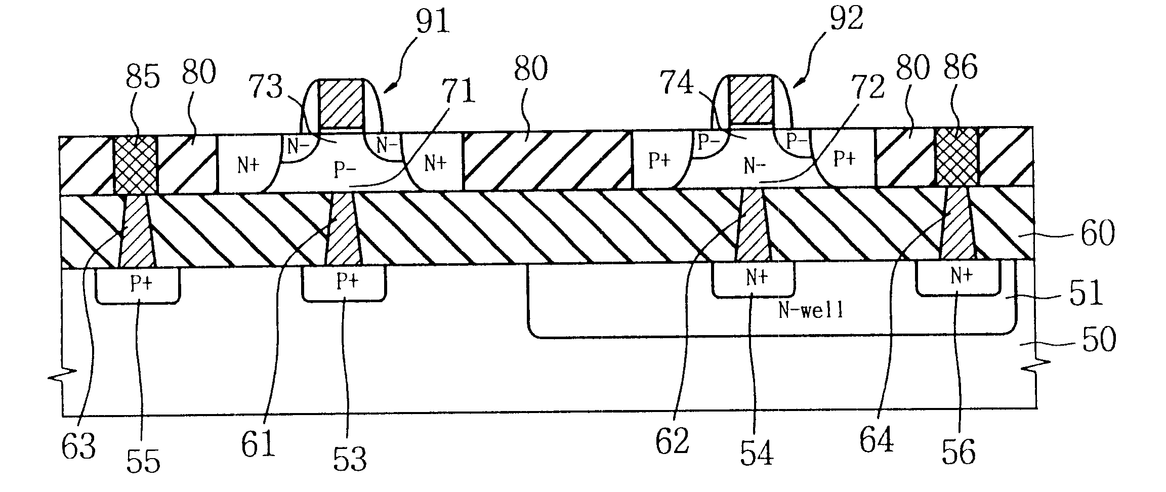
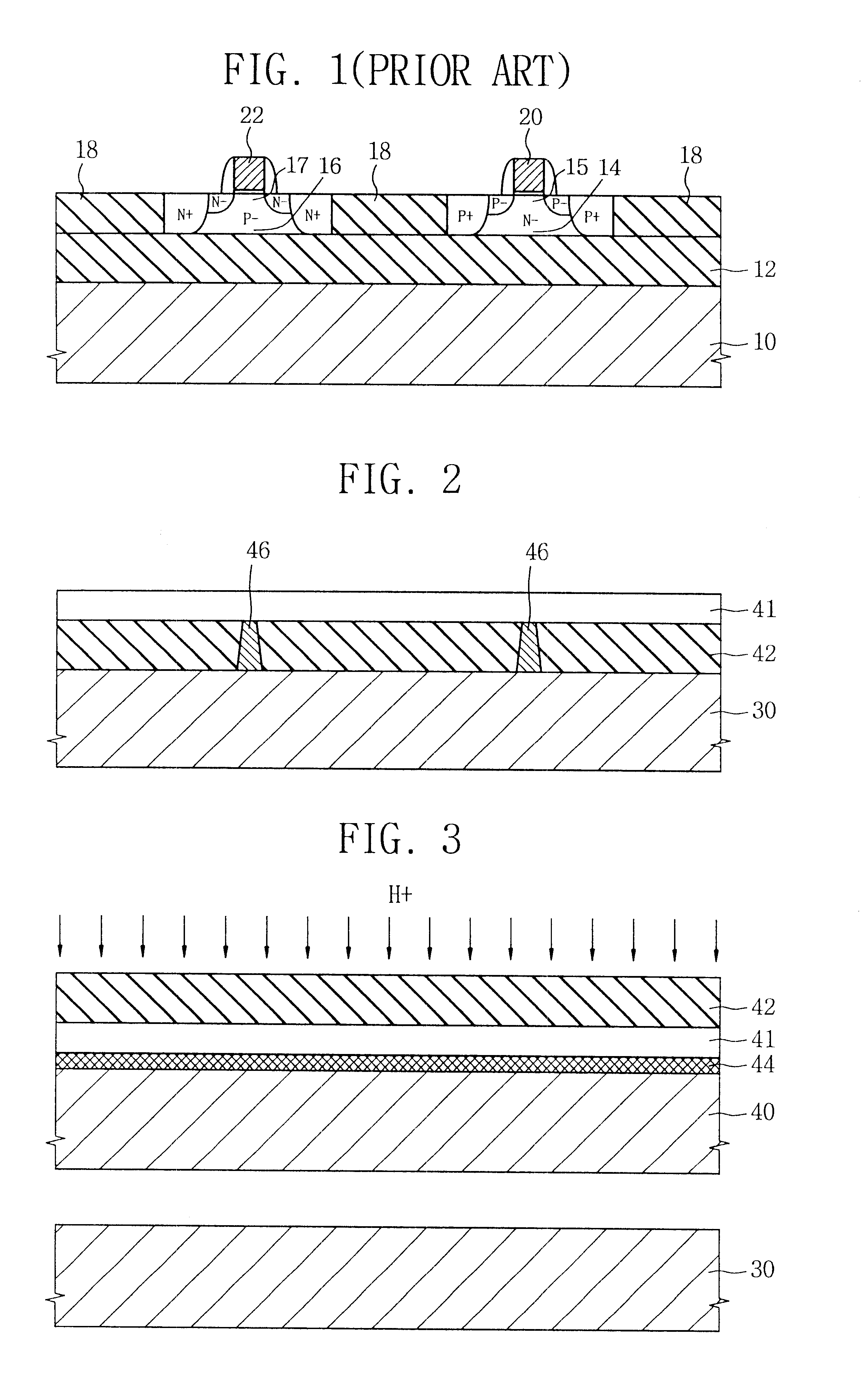
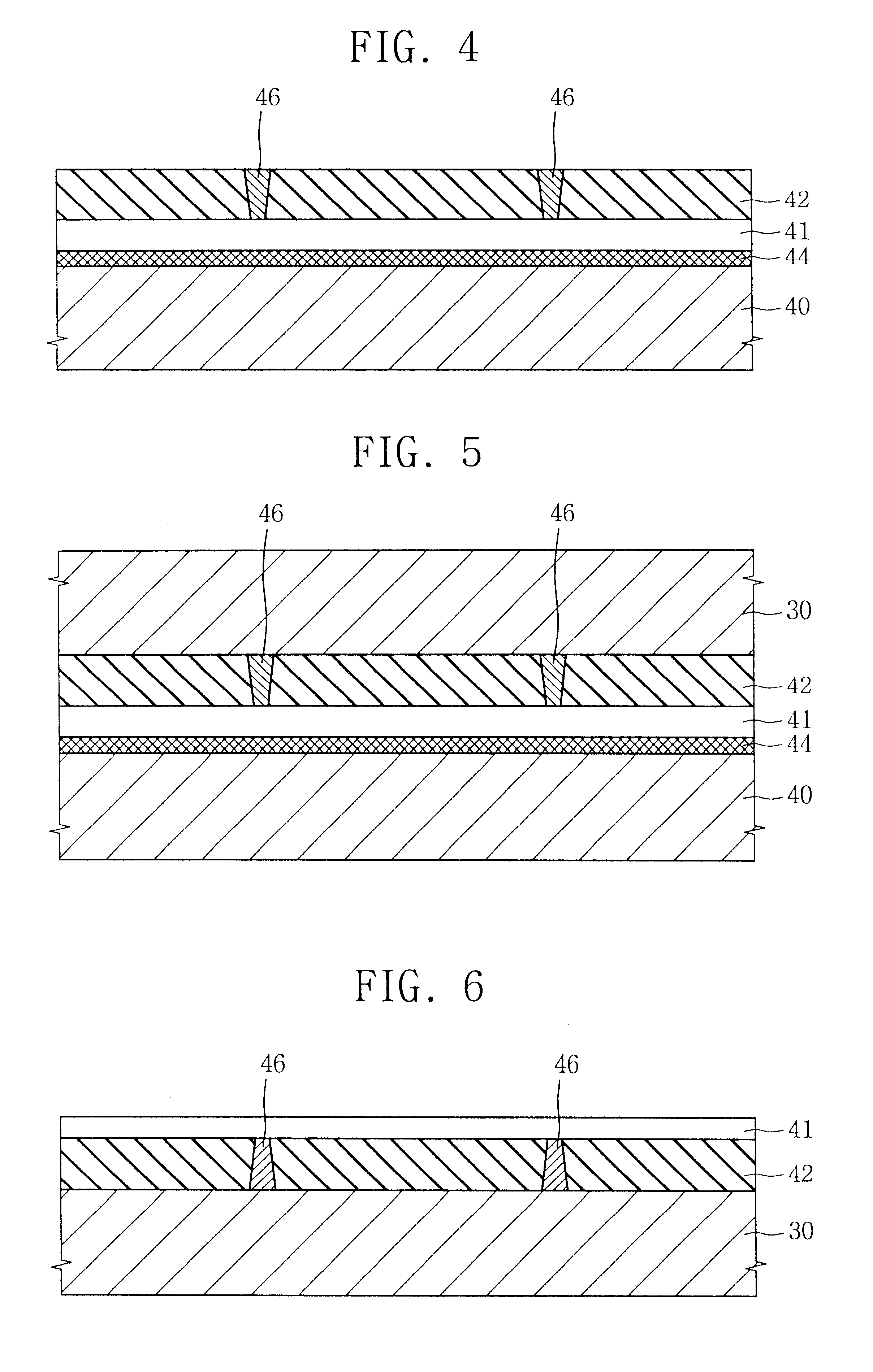
FIG. 2 is a cross-sectional view illustrating the structure of a SOI substrate, and FIGS. 3 through 6 are cross-sectional views illustrating a method for fabricating the SOI substrate in accordance with the present invention. As shown in FIG. 2, the SOI substrate includes a mono-silicon substrate 30, a buried oxide layer 42 formed over the entire surface of the mono-silicon substrate 30, and a thin mono-silicon layer 41 formed over the entire surface of the buried oxide layer 42. Conductive layers 46 are formed at through holes of the buried oxide layer 42 positioned between the predetermined regions of the thin layer 41 and the substrate 30 for body contacts. The conductive layers 46 can be made a heavily doped mono-silicon layer, a poly-silicon layer or a metal layer like tungsten.

A ...


PUM


Abstract

The present invention relates to a silicon-on-insulator (SOI) substrate, a method for fabricating the SOI substrate and a SOI MOSFET using the SOI substrate to easily migrate the design applied to a conventional bulk silicon substrate to the SOI design and to remove a floating body effect. The SOI substrate includes a mono-silicon substrate, a buried oxide layer formed over the surface of the mono-silicon substrate, and a thin mono-silicon layer formed over the surface of the buried oxide layer. Conductive layers are formed at through holes of the buried oxide layer positioned between the predetermined regions of the thin layer and the substrate for body contacts. Therefore, additional layout spaces are not needed for body contacts and the constant body contact resistance can allow the conventional circuit design applied to the bulk silicon substrate to be migrated to the circuit design applied to the SOI substrate without any modifications. Also, a variety of operational failures caused by the floating effect can be eliminated in the SOI substrate. As a consequence, additional effort is not required for designing or verifying the circuit of the present invention, so as to make it possible to construct a highly efficient, but low power consuming system.

Description

1. Field of the InventionThe present invention relates to a silicon-on-insulator (SOI) and more particularly to a SOI substrate, a method for fabricating the SOI substrate and a SOI MOSFET using the SOI substrate to remove a floating body effect without a separate layout space.2. Description of Related ArtIn general, a wide isolation region is required in the process for fabricating complementary metal oxide semiconductor (CMOS) transistors to prevent latch-up of the CMOS transistors and to isolate the transistors. However, the wide isolation region results in larger size and low integration of a semiconductor device. In order to solve the aforementioned problem, a SOI technique has been disclosed to fabricate a SOI transistor, which has proved to be superior to a bulk silicon transistor by providing a lower power consumption rate and in an application to a performance VLSI.FIG. 1 is a schematic cross-sectional view of a conventional SOI CMOS transistor. As shown in FIG. 1, the conv...

Claims


Application Information

Patent Timeline
IPC IPC(8): H01L21/762H01L21/84H01L21/70H01L27/12H01L21/20
CPCH01L21/76254H01L21/76264H01L21/76275H01L21/76283H01L21/84H01L27/1203H01L21/20
Inventor KIM, MIN-SU
Owner SAMSUNG ELECTRONICS CO LTD
Why Eureka
Try Eureka