Method of detecting film defects using chemical exposure of photoresist films

a technology of photoresist film and chemical exposure, applied in the field of semiconductor/solid-state device testing/measurement, instruments, photomechanical equipment, etc., can solve the problems of device failure, defect interference with subsequent lithography processing on the interlevel dielectric layer, and variety of defects during interlevel dielectric and metallization layer processing

Inactive Publication Date: 2002-08-27
SDGI HLDG +1
View PDF0 Cites 12 Cited by
  • Summary
  • Abstract
  • Description
  • Claims
  • Application Information

AI Technical Summary

Problems solved by technology

A variety of defects may arise during processing of interlevel dielectric and metallization layers.
In either case, the defect can interfere with subsequent lithography processing on the interlevel dielectric layer, via etching or conductor deposition.
However, the presence of defects in the surface of an underlying layer may cause the overlying film to later delaminate and lead to device failure.
As an example, undetected surface defects in an interlevel dielectric layer may result in poor contact lithography or etching.
In such circumstances, the time and material involved in the contact lithography, e.g., the photoresist application, exposure, development, and contact etch will be wasted.
A limitation associated with conventional surface defect inspection is tool sensitivity.
Many types of defects are too small for the inspection tool to resolve.
Thus, defects capable of causing device failure may pass inspection if they do not happen to fall within the designated sample portions of the film.
Another limitation associated with some conventional defect inspection methods is destruction of the scanned surface.
Techniques such as transmission electron microscopy and time of flight secondary ion beam spectroscopy can identify certain kinds of defects, but also result in the destruction of the scanned structure.

Method used


Image

  • Method of detecting film defects using chemical exposure of photoresist films
  • Method of detecting film defects using chemical exposure of photoresist films
  • Method of detecting film defects using chemical exposure of photoresist films

Examples


Embodiment Construction

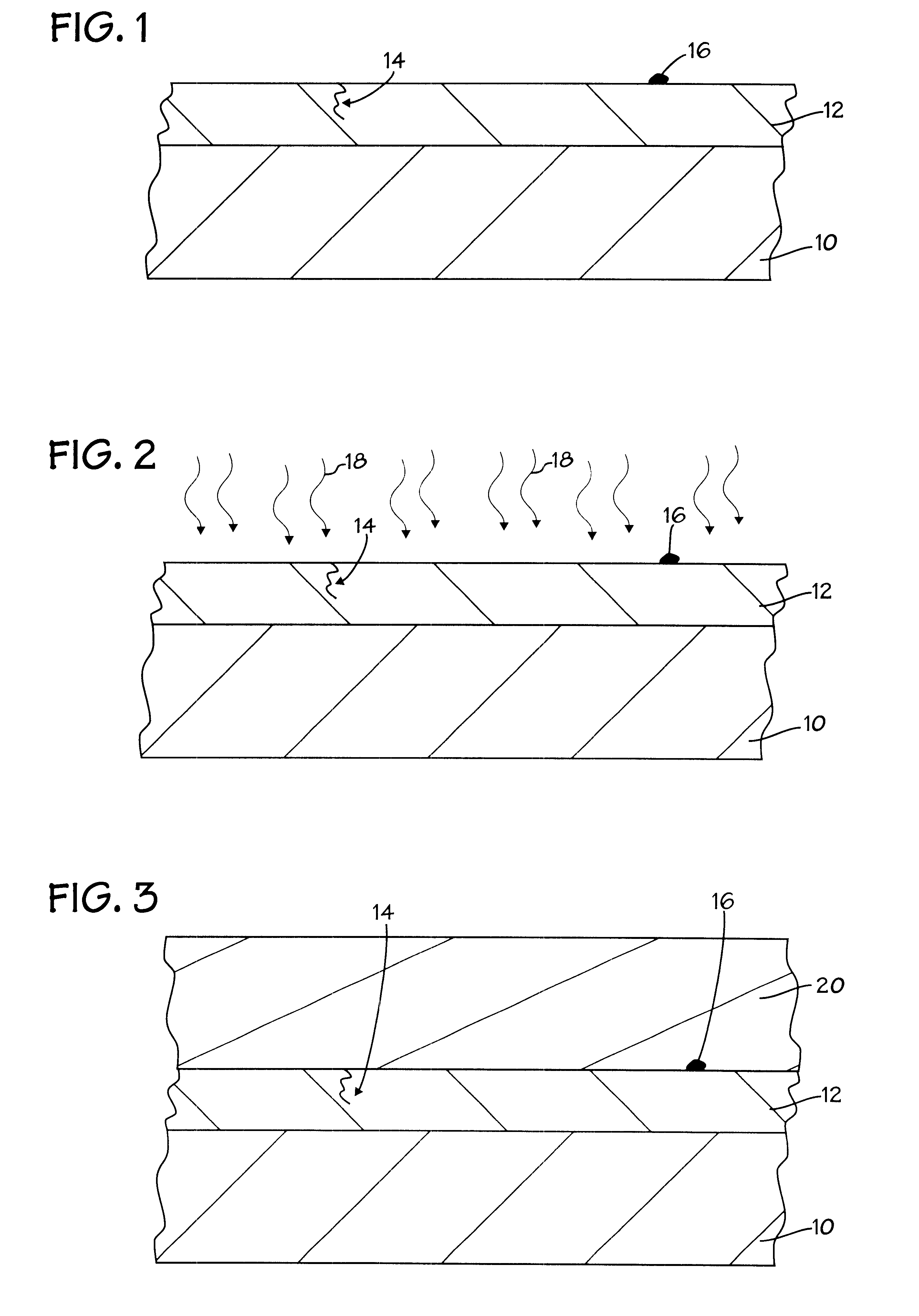
In the drawings described below, reference numerals are generally repeated where identical elements appear in more than one figure. An exemplary method of inspecting a semiconductor workpiece 10 for defects may be understood by referring now to FIGS. 1-8 and initially to FIG. 1. FIG. 1 depicts a cross-sectional view of a small portion of the a semiconductor workpiece 10 upon which a semiconductor processing film 12 is formed. The workpiece 10 may be a semiconductor wafer or other type of substrate used in circuit fabrication and may be composed of silicon, silicon-on-insulator or other widely used substrate materials. The processing film 12 may be any of a variety of films used in semiconductor processing, such as, for example, oxide, silicon nitride, silicon oxynitride, polycrystalline or amorphous silicon or the like. For the purposes of the present illustration, the film 12 is an oxide film of the type used as interlevel dielectric layers.

As the skilled artisan will appreciate, t...


PUM

PropertyMeasurementUnit
thicknessaaaaaaaaaa
thicknessaaaaaaaaaa
thicknessaaaaaaaaaa

Abstract

Various methods of inspecting a semiconductor workpiece for defects are provided. In one aspect, a method of inspecting a surface of a semiconductor workpiece for defects is provided that includes applying a negative-tone photoresist film to the surface and baking the negative-tone photoresist film to release solvent therefrom and to facilitate release of catalyzing substances held by the defects into the negative-tone photoresist film. The catalyzing substances react chemically with at least one moiety of the photoresist film to thereby lower the solubility of one or more portions of the negative-tone photoresist film in a developer. The negative-tone photoresist film is developed with the developer and the surface is inspected for the portions of the negative-tone photoresist film remaining after the developing process. The remaining portions of the negative-tone photoresist film are indicative of the locations of the defects.

Description

1. Field of the InventionThis invention relates generally to semiconductor processing, and more particularly to methods of inspecting semiconductor workpieces for surface defects using chemical exposure of resist films.2. Description of the Related ArtLarge scale integrated circuits now routinely contain millions of individual transistors and other electronic components. Most of the interconnections for the numerous individual components are provided via one or more metallization layers that serve as global interconnect levels. Each metallization layer is ordinarily deposited on the substrate of the integrated circuit as a single continuous layer that is thereafter patterned lithographically and etched to remove metal from areas where metal lines are not required.In addition to the one or more metallization layers, modern integrated circuits also incorporate numerous routing-restricted interconnect levels commonly known as local interconnects and contacts. Local interconnects and co...

Claims


Application Information

Patent Timeline
Patent Type & Authority Patents(United States)
IPC IPC(8): G01N21/95G01N21/91G01N21/88G03F7/00H01L21/66
CPCG01N21/91G01N21/9501G03F7/00H01L22/24G01N21/9505
Inventor SUTTON, DANIEL E.LANSFORD, CHRISTOPHER H.
Owner SDGI HLDG
Why Eureka
Try Eureka