

Apparatus improving latchup immunity in a dual-polysilicon gate
- Summary
- Abstract
- Description
- Claims
- Application Information
AI Technical Summary
Benefits of technology
Problems solved by technology
Method used
Image

Examples
Embodiment Construction
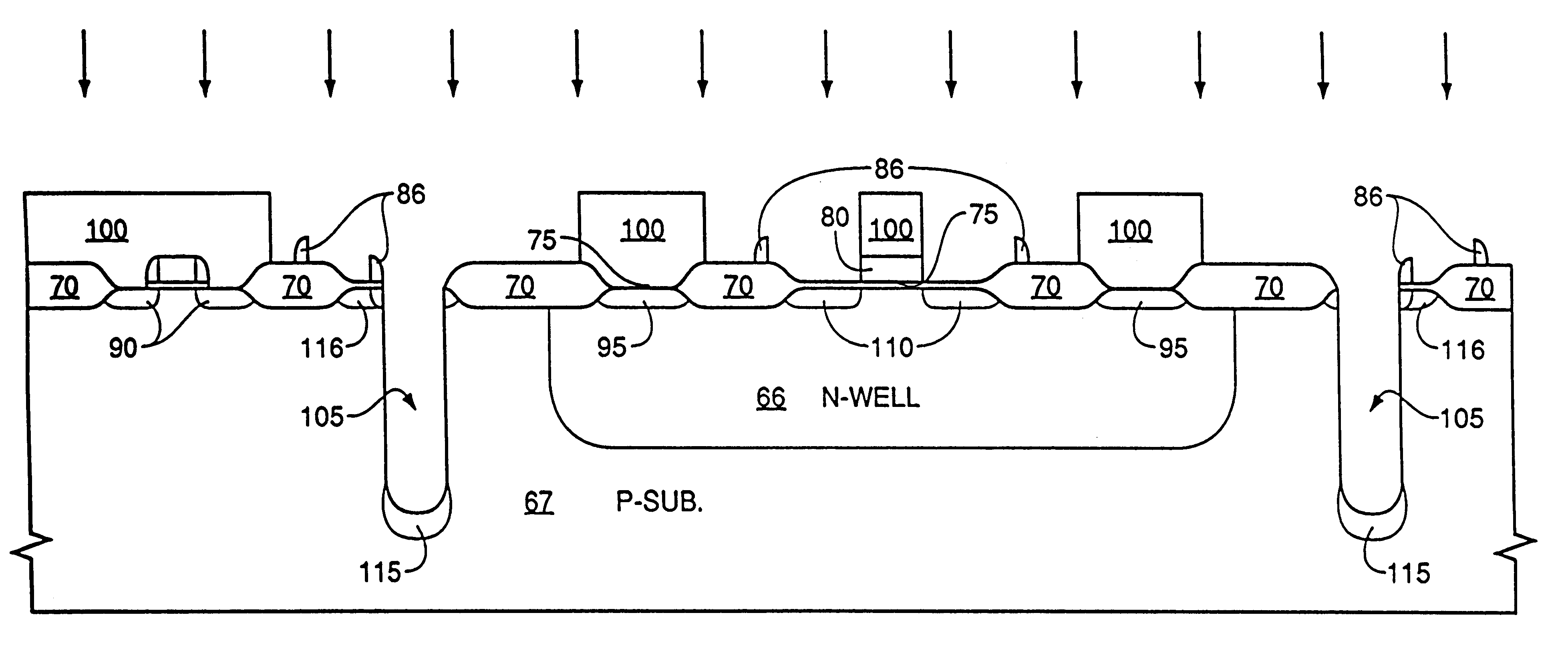
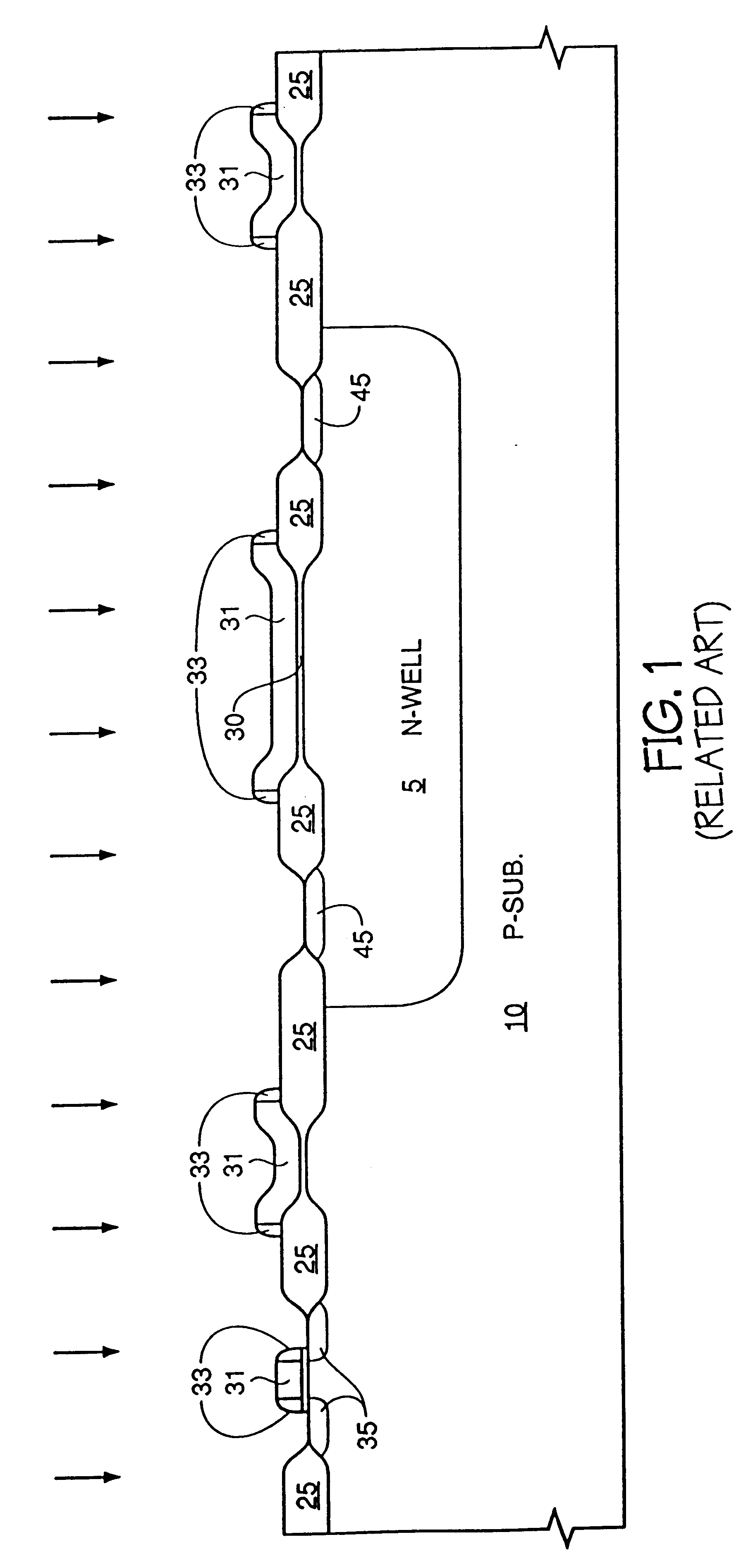
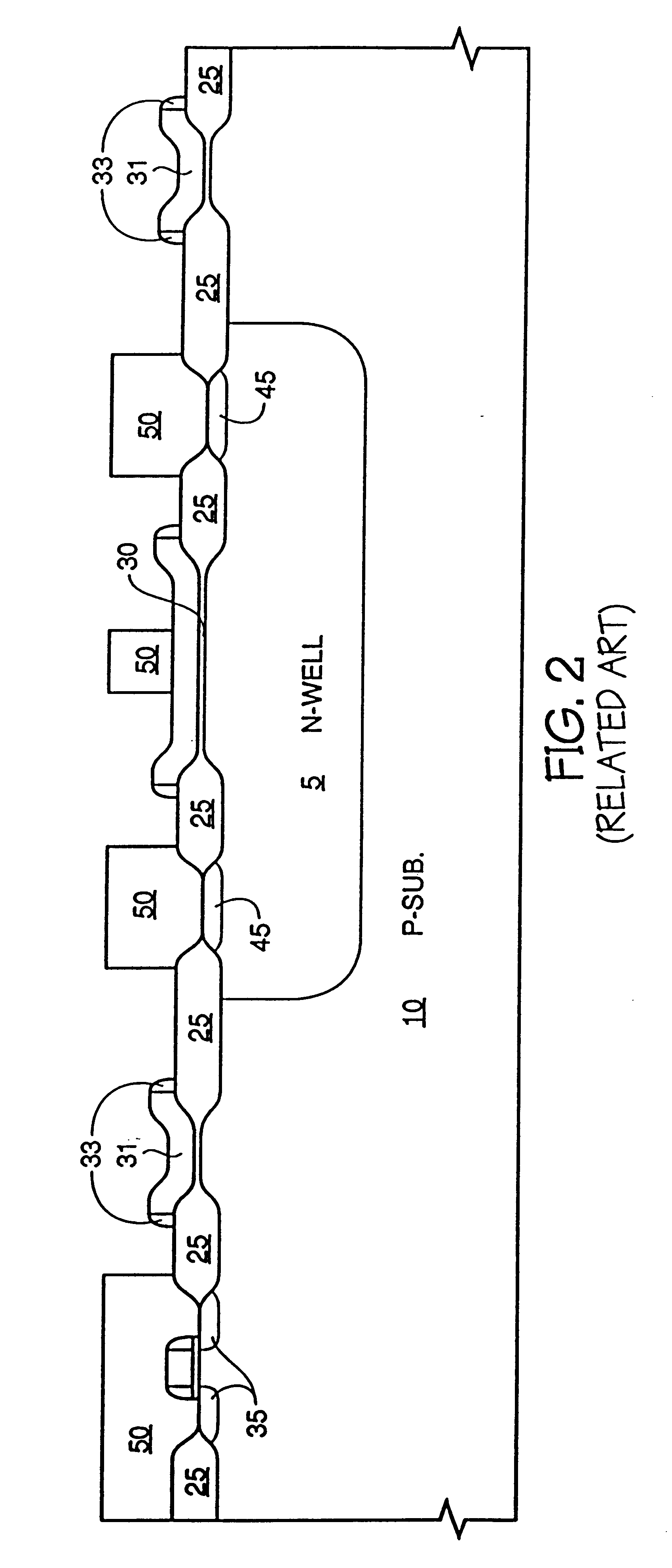
The invention is a method for creating a portion of an integrated circuit on a semiconductor wafer. In the method of the invention an isolation trench and an isolation region are formed in order to electrically isolate two regions of the integrated circuit from each other. The isolation trench and the isolation region minimize undesired effects, such as latch up caused by the actuation of parasitic bipolar transistors.
Although the method of the invention pertains to the fabrication of the isolation trench and the isolation region of the integrated circuit, the method will be described in conjunction with the formation of transistors in order to provide a clearer picture of the function of the invention.
Referring to FIGS. 4A-C, an N-well 66 is formed in a P-substrate 67. Creating an N-well within a P-type substrate is well known to those skilled in the art and involves doping the substrate with impurity atoms to create a negatively doped region in which to fabricate a P-channel metal...
PUM
 Abstract
Description
Claims
Application Information