Color liquid crystal display panel

a liquid crystal display panel and liquid crystal display technology, applied in the field of color liquid crystal display panels, can solve the problems of resin film falling off, black resin film easily falling off the insulation film, and difficult to enhance the fineness of the panel

Inactive Publication Date: 2002-09-03
NEC LCD TECH CORP
View PDF15 Cites 31 Cited by
  • Summary
  • Abstract
  • Description
  • Claims
  • Application Information

AI Technical Summary

Benefits of technology

According to the present invention, a contacting color layer including at least one color layer selected from the group consisting of the first to third color layers is provided between the black matrix and the insulation film. As to the color layers, since light even passes through the inside of the color layers during fabrication of the color layers by photolithography, the color layer is sufficiently sensitized, and therefore, contact between the color layer and the insulation film is tight. As to the black matrix, high optical density is obtained since at least one of the color layers is disposed under the black matrix, and therefore, the black matrix can be formed to be thin. Moreover, since the base materials of the black matrix and the color layers are usually the same, e.g., an acrylic resin, contact between the color layers and the black matrix is also high. As a result, tight contact between the black matrix and the insulation film is achieved. Since this suppresses peeling of the black resin film, which serves as the raw material of the black matrix, fine patterning is possible during development, and high fineness is accordingly realized. In addition, since the color layers disposed under the black matrix as well serve as a light shielding layer in addition to the black matrix, high optical density is obtained.

Problems solved by technology

However, since such a structure demands large margins for a black matrix which is disposed between adjacent inter-pixel opening portions to improve contrast, it is difficult to enhance the fineness of the panel with this structure.
Since the width used under the optimal condition for development (development margin) of the black resin film is extremely narrow, there is a problem in that the black resin film easily falls off the insulation film 109 while being developed.
The black resin film falls off because the black resin film at its surface portions absorbs light during patterning by photolithography and thus fails to be sensitized inside.
Although improvement is possible to a certain extent if the black resin film is formed as a thin film, this solution leads to a new problem of lowered optical density.
Further, in an effort to increase an optical density, an increased carbon content results in a trade off in that a ratio of an acrylic component, which contributes to a tight contact with the underlying member, decreases and hence a contact capability decreases.
This is another problem in that it is difficult to enhance optical density, namely, light shielding capability for the purpose of obtaining excellent contrast.
However, even if such a laminated member is used on a TFT-side glass substrate as an alternative to a black matrix, sufficient shielding of light is not achieved, and therefore, the OD value decreases and contrast accordingly decreases.
However, in such a color filter, since a light shielding rate becomes different depending on the color of the adjacent color layer, the contrast of a displayed image varies, and hence, the image appears uneven.

Method used


Image

  • Color liquid crystal display panel
  • Color liquid crystal display panel
  • Color liquid crystal display panel

Examples


Embodiment Construction

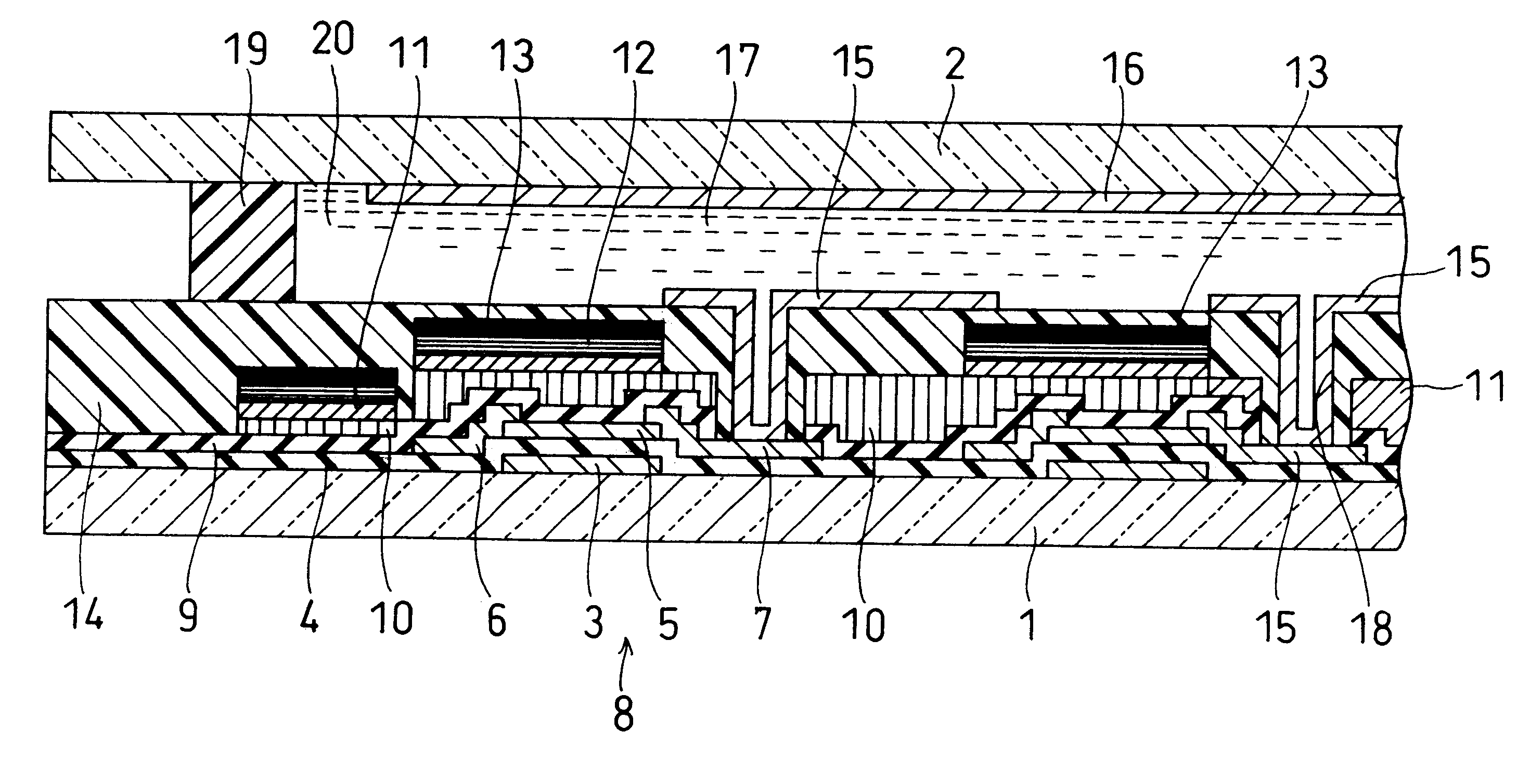
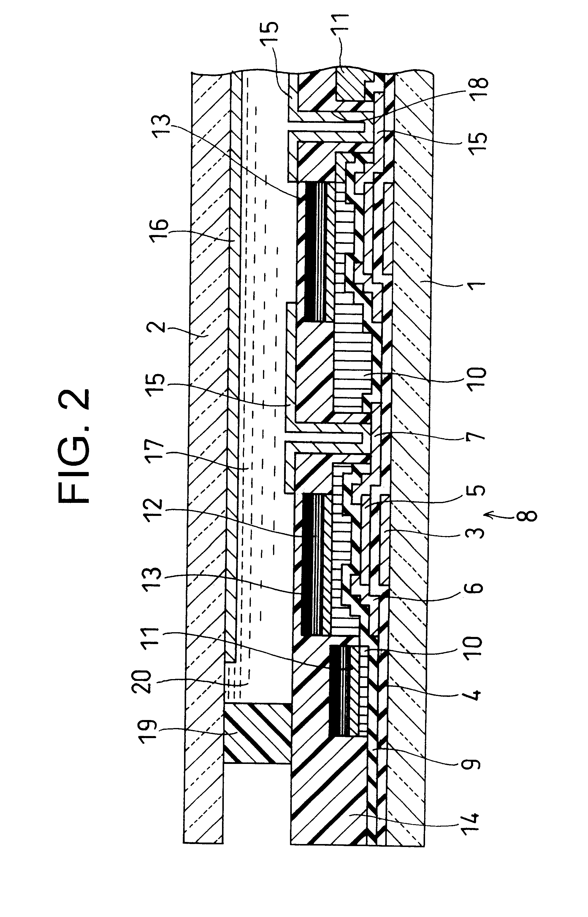
In the following, preferred embodiments of the present invention will be specifically described with reference to the attached drawings. FIG. 2 is a cross sectional view showing a structure of a color liquid crystal display panel according to an embodiment of the present invention.

In the color liquid crystal display panel according to the present embodiment, a liquid crystal layer 17 is disposed between a TFT-side glass substrate 1 and a counter glass substrate 2. In the following, the closer sides to the liquid crystal layer 17 of the glass substrates 1 and 2 will be referred to as "the inner sides" and the opposite sides will be referred to as "the outer sides."

A plurality of gate electrodes 3 are formed on the inner-side surface of the TFT-side glass substrate 1, and a gate insulation film 4 is formed so as to cover the gate electrodes 3. The gate electrodes 3 of a plurality of TFTs 8 which define rows are connected in common to gate lines (not shown) which extend in the row dire...


PUM

PropertyMeasurementUnit
ODaaaaaaaaaa
thicknessaaaaaaaaaa
thicknessaaaaaaaaaa

Abstract

First and second transparent substrates which are arranged to face each other are provided to a color liquid crystal display panel. A liquid crystal layer is provided between the first and the second transparent substrates. A plurality of thin film transistors are provided on the first transparent substrate. An insulation film provided on the first transparent substrate so as to cover the thin film transistors. A color filter which includes first to third color layers stacked on the insulation layer is provided. A contacting color layer is provided on the insulation film in a region above the thin film transistors. The contacting color layer has at least one color layer selected from a group of composed of the first to third color layers. A black matrix is provided on the contacting color layer. The black matrix has opening portions for transmitting light from the color filter.

Description

1. Field of the InventionThe present invention relates to a color liquid crystal display panel which comprises thin film transistors, and more particularly, to a color liquid crystal display panel in which tight contact between a black matrix and an underlying member is improved so as to achieve high fineness.2. Description of the Related ArtA color liquid crystal display panel comprises two glass substrates and a liquid crystal layer which is disposed between the glass substrates. In general, in a panel of the thin film transistor (TFT; Thin Film Transistor) type, color layers of three colors (red, green and blue) are formed on a counter glass substrate which is faced with a TFT-side glass substrate which seats TFTs. However, since such a structure demands large margins for a black matrix which is disposed between adjacent inter-pixel opening portions to improve contrast, it is difficult to enhance the fineness of the panel with this structure.Against this background, a color liqui...

Claims


Application Information

Patent Timeline
Patent Type & Authority Patents(United States)
IPC IPC(8): G02F1/1335G02F1/13G02F1/1362H04N5/66G03F7/004G09F9/30H04N9/30
CPCG02F1/133514G02F1/136209G02F1/136227G02F2001/136222G02F1/136222G02F1/1335
Inventor YAMAMOTO, YUJIOKAMOTO, MAMORUSAKAMOTO, MICHIAKIWATANABE, TAKAHIKOKIKKAWA, HIRONORIMARUYAMA, MUNEO
Owner NEC LCD TECH CORP
Why Eureka
Try Eureka