
Memory system using FET switches to select memory banks

a memory system and switch technology, applied in the direction of memory adressing/allocation/relocation, digital storage, instruments, etc., can solve the problems of increasing the delay in the circuit path, increasing the difficulty of silicon implementation of high speed and high density, and in some cases, prohibitiv

Inactive Publication Date: 2002-09-03
FOOTHILLS IP LLC
View PDF5 Cites 215 Cited by
  • Summary
  • Abstract
  • Description
  • Claims
  • Application Information

AI Technical Summary

Benefits of technology

It is the general object of the current invention to provide a DDR memory architecture using SDR memory chips. It is a further object of this invention to combine DDR memory chips to provide a quad-speed output.

Problems solved by technology

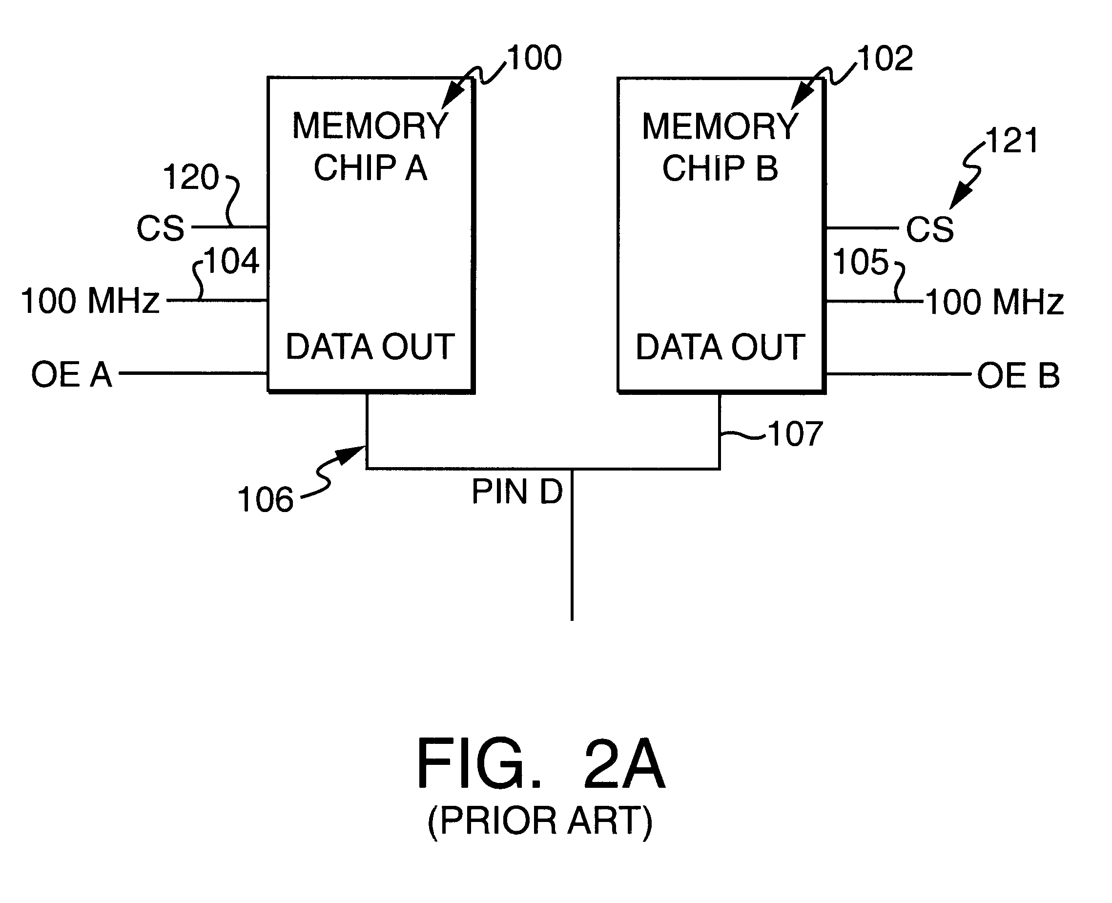
Density and speed interfere with each other, When the density increases, the speed decreases simply because many levels of interconnection are required for the circuitry and thus more delay is introduced to the circuit path.
Also the implementation of high speed and high density within the silicon becomes very difficult, and in some cases, prohibitive.
The problem appears when one is trying to produce devices that operate at 200 MHz base clock frequency.
Such high speed memory chips are expensive and difficult to produce.

Method used


Image

  • Memory system using FET switches to select memory banks
  • Memory system using FET switches to select memory banks
  • Memory system using FET switches to select memory banks

Examples


embodiment

WITHOUT PHASE DELAYED CLOCK

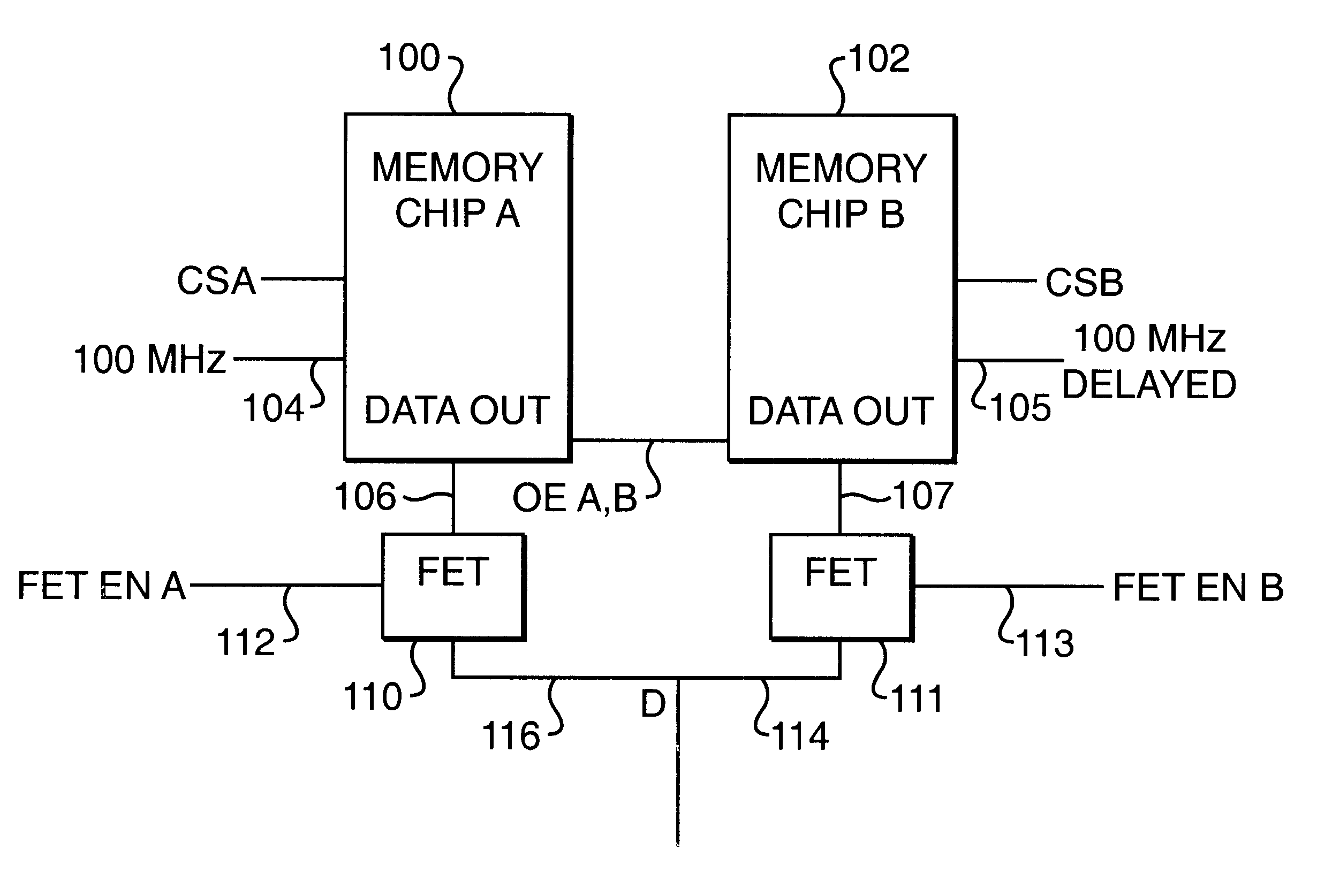
In a final preferred embodiment, memory banks A and B are both DDR memories. The same basic clock signal is used to synchronize both memory bank A and memory bank B.

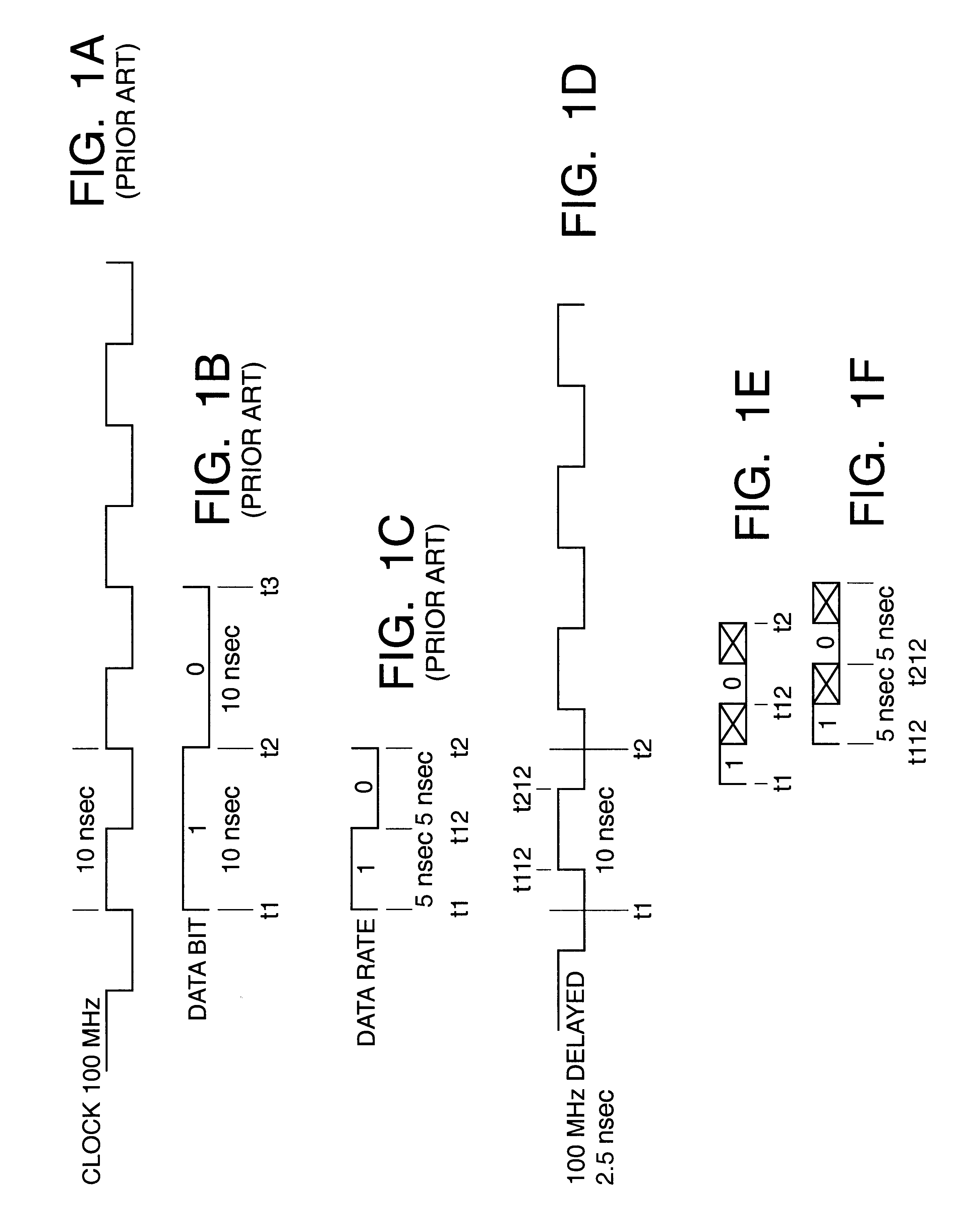
At the beginning of each cycle, memory bank A produces a first internal output which is valid for a duration p / 4 of the basic clock cycle, and a second internal output at p / 2 after the beginning of the cycle, again lasting for a duration p / 4. Memory bank B produces a third internal output, beginning at p / 4 after the beginning of the cycle. which is valid for a duration p / 4 of the basic clock cycle, and a fourth internal output, again at 3p / 4 after the beginning of the cycle, again lasting for a duration p / 4.

Before outputting these internal outputs onto the data bus, the first and second internal outputs are exchanged, and the third and fourth internal outputs are exchanged. As a result, the data on the data bus will contain the data bits from memory chip A during the first half of the clock per...


PUM


Abstract

A computer memory system provides a double data rate (DDR) memory output while requiring memory chips with only half the frequency limit of the prior art DDR memory chips. The system contains a first memory bank having data lines and a second memory bank having data lines. The first and second memory banks are associated with first and second clock signals, respectively, where the second clock signal is delayed from the first clock signal such that the data lines of the first memory bank are connected to a data bus in synchronism with the first clock signal while the data lines of the second memory bank are connected with the data bus in synchronism with the second clock signal. In one embodiment, a first FET switch connects the data lines of the first memory bank with the data bus and a second FET switch connects the data lines of the second memory bank with the data bus. The second FET switch is connected to the data bus at a time delayed from the beginning after the start of each clock cycle of the second clock signal. As a result, the data bus is never connected to the data lines of both memory banks at the same time, but rather, the data bus is alternately connected with the first memory bank and then the second memory bank.

Description

The present invention relates to providing increased data access speed in computer memories without increasing the basic clock rate of the memory.DESCRIPTION RELATIVE TO THE PRIOR ARTTerminologyThroughout this description the following terms are used:DIMM=Dual In line Memory ModuleSDRAM=Synchronous Dynamic Random Access Memory.DDR=Double Data Rate. Data bit duration equals one half the period of the clock frequency. Two bits of data are used in one period of the base clock. See FIG. 1(b).DBR=Double Bus Rate.SDR=Single Data Rate.DBF=Data Bit Frequency. The number of bits per second per pin. Referred to as xx bit / sec / pin.DR =Data Rate. The Data Bit duration equal to one period of the base clock. See FIG. 1(a)Definition: Double Bus Rate (DBR)For the purpose of description through out this document, the term DBRTM (Double Bus Rate) will be used. Double Bus Rate means that the Data Rate. out of and into a BUS system will be double of what each individual chip connected to the BUS deliver...

Claims


Application Information

Patent Timeline
Patent Type & Authority Patents(United States)
IPC IPC(8): G06F13/42G06F12/00G11C7/10
CPCG06F13/4243G11C7/10G11C7/1042
Inventor KARABATSOS, CHRIS
Owner FOOTHILLS IP LLC
Learn More