Metalization of electronic semiconductor devices

a technology of electronic semiconductors and metalization, applied in semiconductor devices, semiconductor/solid-state device details, electrical devices, etc., can solve the problems of imposing a limit on the minimum hemt source-drain spacing, high contact resistance values, and difficult adhesion of contacts, so as to avoid material deterioration

Inactive Publication Date: 2002-09-10
THE UNITED STATES OF AMERICA AS REPRESENTED BY THE SECRETARY OF THE NAVY
View PDF2 Cites 84 Cited by
  • Summary
  • Abstract
  • Description
  • Claims
  • Application Information

AI Technical Summary

Benefits of technology

Another object of this invention is a process for forming a metallized semiconductor elec

Problems solved by technology

However, in such contact schemes for the AlSb/InAs meterials, the contact resistance values are commonly high and the contacts are difficult to adhere.
With such schemes, there is significant lateral diffusion into the channel as a result of rapid thermal annealing, which imposes a limit on the minimum HEMT source-drain spacing.
Although improvements have been made in recent years, the material growth and

Method used


Image

  • Metalization of electronic semiconductor devices
  • Metalization of electronic semiconductor devices
  • Metalization of electronic semiconductor devices

Examples


example 1

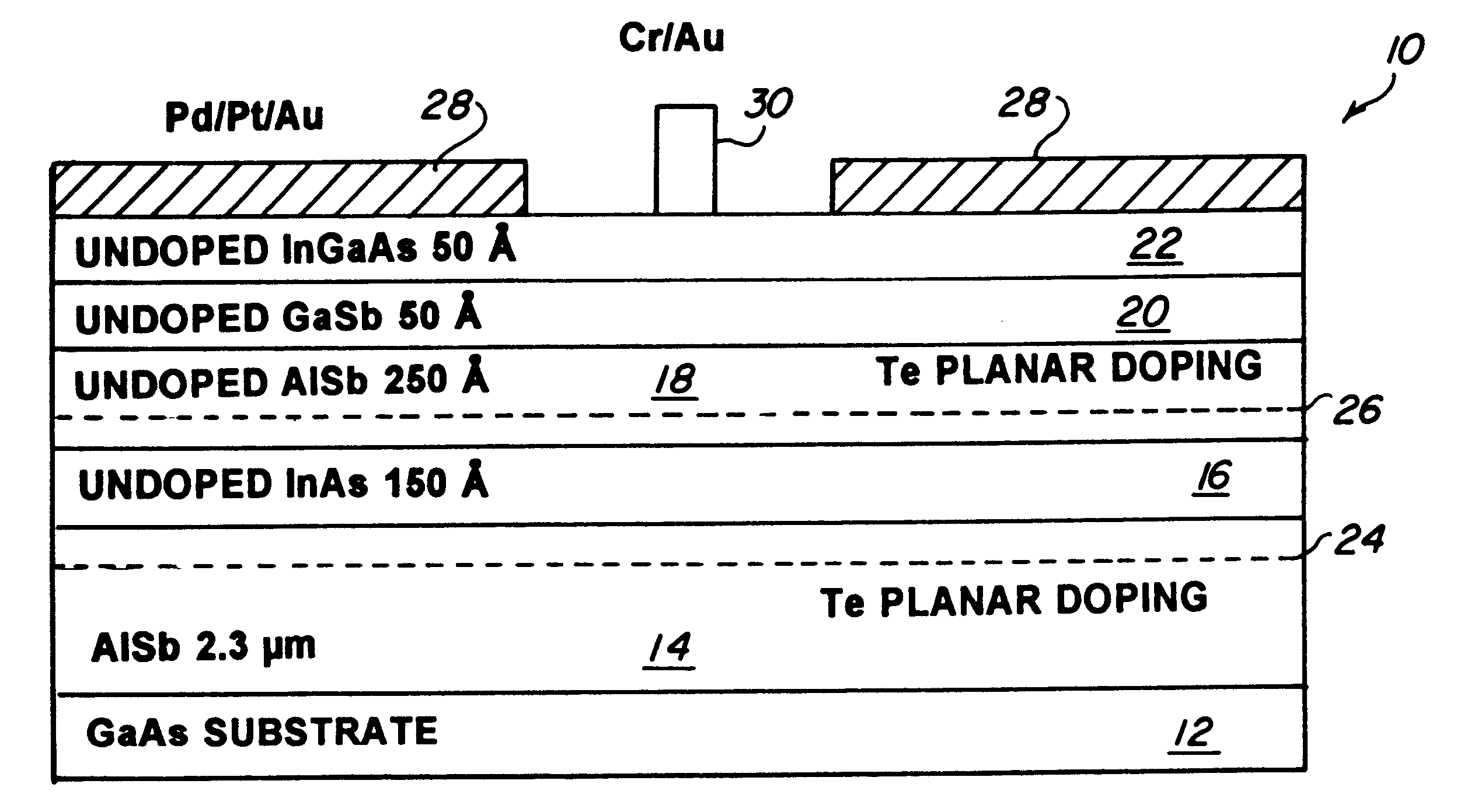
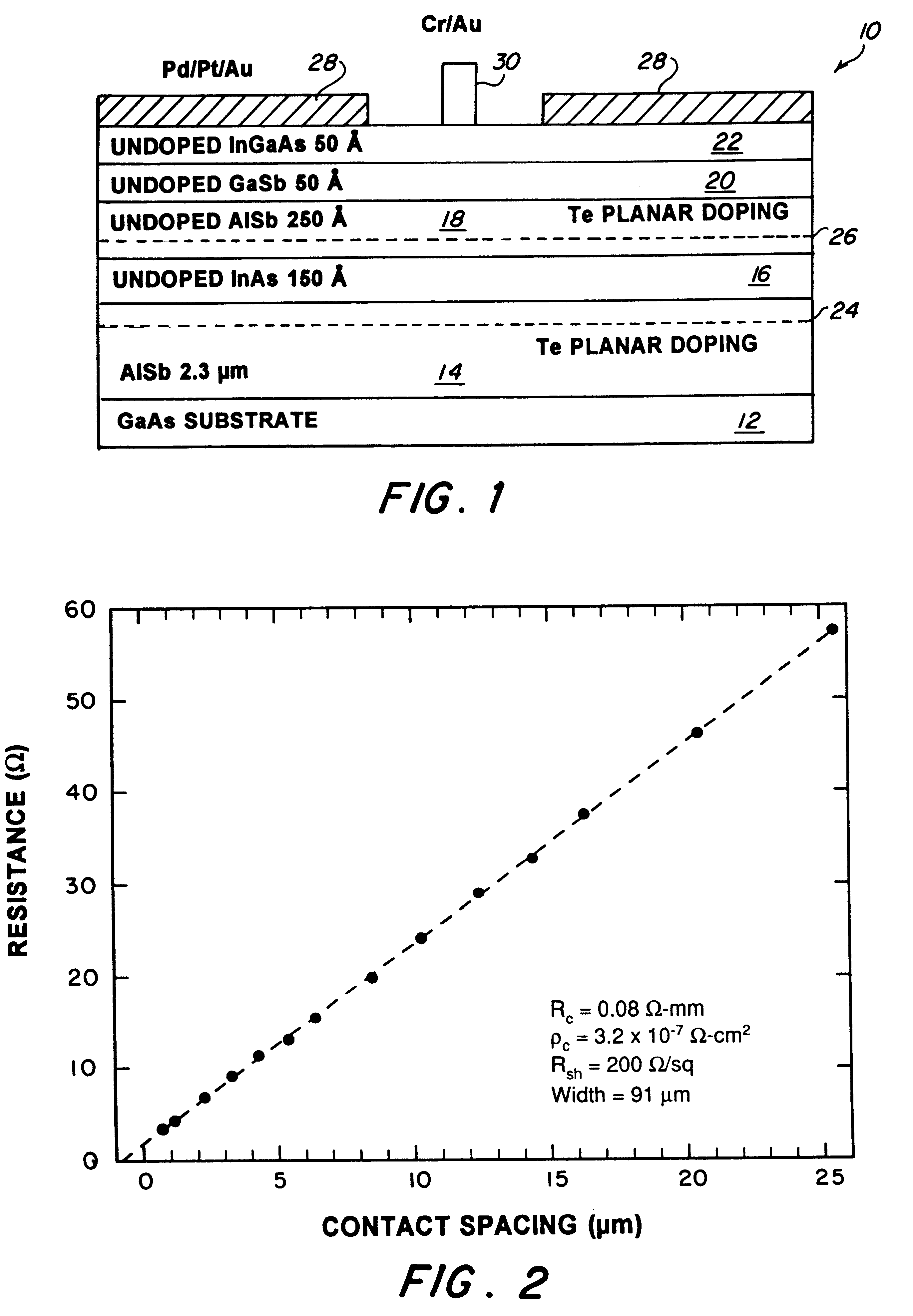
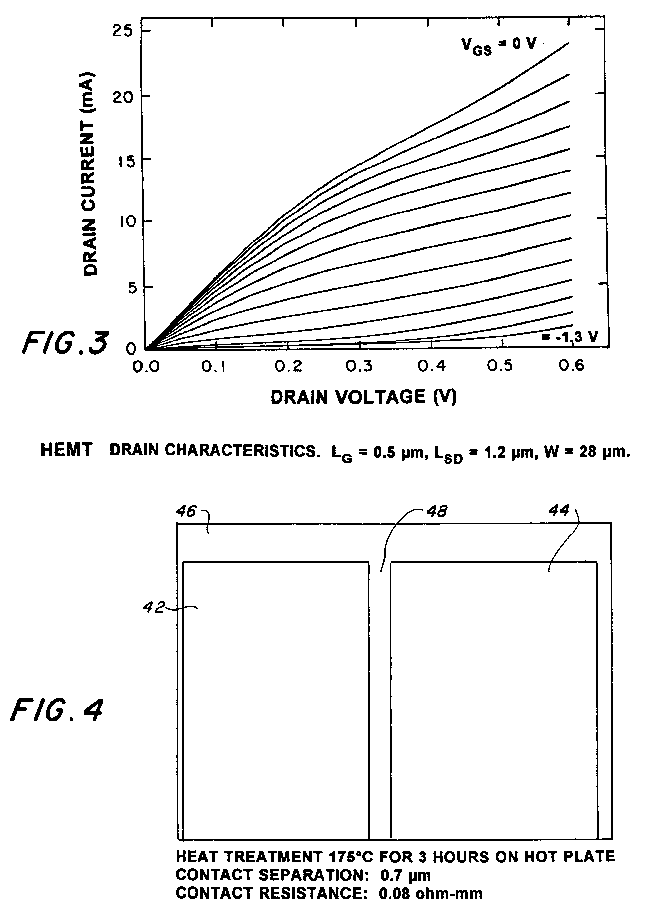
This example demonstrates certain advantages realized in conjunction with a AlSb / InAs-based HEMT provided with a contact of Pd / Pt / Au which was heat treated at 175.degree. C. before provision of the gate.

Pursuant to the disclosure herein, layers of AlSb / InAs 10 were grown my molecular beam epitaxy at 510.degree. C. on an updoped (100) GaAs substrate 12 that was about 400 microns thick. The material layer composition and thickness of the HEMT fabricated using the Pd / Pt / Au ohmic contact metalization scheme is shown in FIG. 1. The 2.3 micron updoped AlSb buffer layer 14, disposed on substrate 12, was used to accommodate the 7% lattice mismatch. Undoped InAs channel or quantum well 16, disposed on layer 14, was 150.ANG. thick; another undoped AlSb layer 18, disposed on layer 16, was 250.ANG. thick; undoped GaSb layer 20, disposed on layer 18, was 50.ANG. thick; and undoped InGaAs layer 22, disposed on layer 20 was also 50.ANG. thick. The electron carriers were supplied by the two Te plan...

example 2

This example is similar to Ex. 1 except that the contact was Pd / Au (100.ANG. / 600.ANG.) and the heat treating step was carried out at 175.degree. C. for 5 hours.

Without the platinum diffusion barrier layer, the gold of the Pd / Au contact exhibited significant lateral diffusion into the channel as a result of the heat treatment at 175.degree. C. for 5 hours.

example 3

This example is similar to Ex. 1 except that the heat treatment was carried out in one instance at 175.degree. C. for 5 hours and in another instance it was carried out at 250.degree. C. for 19 hours.

When the heat treatment was carried out at 175.degree. C. for 5 hours, the contact resistance was 0.1 ohm-mm whereas when the heat treatment was at 250.degree. C. for 19 hours, no significant change in the contact resistance or the sheet resistance was observed. On the basis of scanning electron microscopy, no reaction was observed in the region adjacent to the contact as a result of the heat treatment at 250.degree. C. for 19 hours.


PUM


Abstract

An electronic semiconductor device comprising a semiconductor base deposited on a semiconductor substrate by means of molecular beam epitaxy and source, drain and gate disposed on the base in a spaced relationghip to each other, the source and the drain comprising Pd/barrier/Au layers with the palladium layer being in contact with the device. The device is fabricated conventionally except the heat treating is at above about 170° C. for ¼-10 hours sufficient for the palladium layer to react with the base yielding reduced contact and access resistances and a narrower spacing between source and drain.

Description

BACKGROUND OF INVENTION1. Field of InventionThis invention pertains to metalization of electronic semiconductor devices.2. Description of Prior Artthe AuGe / Ni / Au and AuGe / Au metalization schemes are commonly used in GaAs-based and InP-based devices. Also, the most commonly reported source-drain contacts for AlSb / InAs-based semiconducting materials have been AuGe / Ni / Au or AuGe / Au. However, in such contact schemes for the AlSb / InAs meterials, the contact resistance values are commonly high and the contacts are difficult to adhere. With such schemes, there is significant lateral diffusion into the channel as a result of rapid thermal annealing, which imposes a limit on the minimum HEMT source-drain spacing. Furthermore, scanning electron microscopy revealed that a region of the semiconducting material reacted, as a result of the heat treatment, and extended laterally inwardly from each contact edge.Semiconducting devices fabricated using the AlSb / InAs-based material systems have potent...

Claims


Application Information

Patent Timeline
IPC IPC(8): H01L21/02H01L29/778H01L29/02H01L21/285H01L21/335H01L29/207H01L29/66
CPCH01L21/28575H01L29/207H01L29/66462H01L29/7785
Inventor BOOS, JOHN BRADLEY
Owner THE UNITED STATES OF AMERICA AS REPRESENTED BY THE SECRETARY OF THE NAVY
Why Eureka
Try Eureka