Method of manufacturing a trench gate power transistor with a thick bottom insulator

a technology of trench gate power transistor and thick bottom, which is applied in the direction of semiconductor devices, diodes, electrical devices, etc., can solve the problems of reducing the performance of trench power transistor, difficult to form shallow junctions, and affecting so as to improve the gate insulation pressure resistance improve the drive capability and improve the effect of trench power transistors

Inactive Publication Date: 2002-09-24
HITACHI LTD +1
View PDF4 Cites 75 Cited by
  • Summary
  • Abstract
  • Description
  • Claims
  • Application Information

AI Technical Summary

Benefits of technology

A general object of the present invention is to provide a technology which can decrease a capacity between the gate and drain in the trench power transistor.
It is a more specific object of the present invention to provide a technology which can improve the trench power transistor's drive capability.
It is another object of the present invention to provide a technology which can improve the gate insulation pressure resistance of the trench power transistor.
It is still another object of the present invention to provide a technology which can form a shallow junction for the source region in the trench power transistor.
It is a further object of the present invention to provide a technology which can improve controllability of the source region and the channel region in the trench power transistor.
It is a still further object of the present invention to provide a technology which can improve the trench power transistor performance.

Problems solved by technology

However, the inventors found the following problems in the technology disclosed in the above-mentioned publication.
Therefore, there is a problem that impurities in the source-drain drain region may diffuse during heat treatment or the like to follow using the silicon nitride film as an oxidation-resistant mask.
It is difficult to form a shallow junction in the source region.
As it is difficult to set and control a channel length for the trench power transistor, there arises a problem of degrading the trench power transistor performance.

Method used


Image

  • Method of manufacturing a trench gate power transistor with a thick bottom insulator
  • Method of manufacturing a trench gate power transistor with a thick bottom insulator
  • Method of manufacturing a trench gate power transistor with a thick bottom insulator

Examples


first embodiment

[First Embodiment]

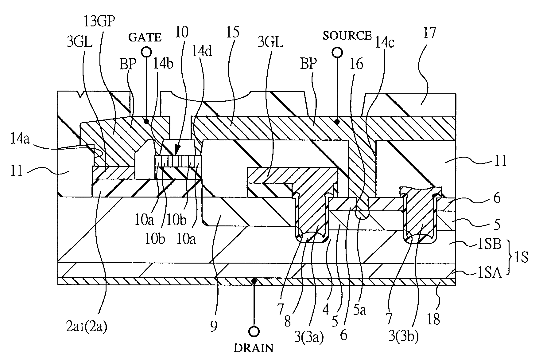
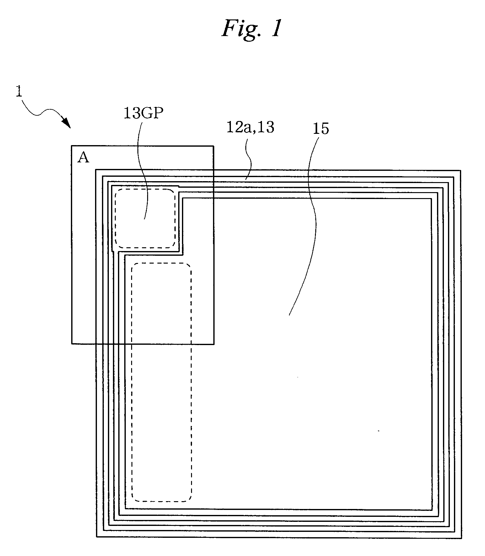
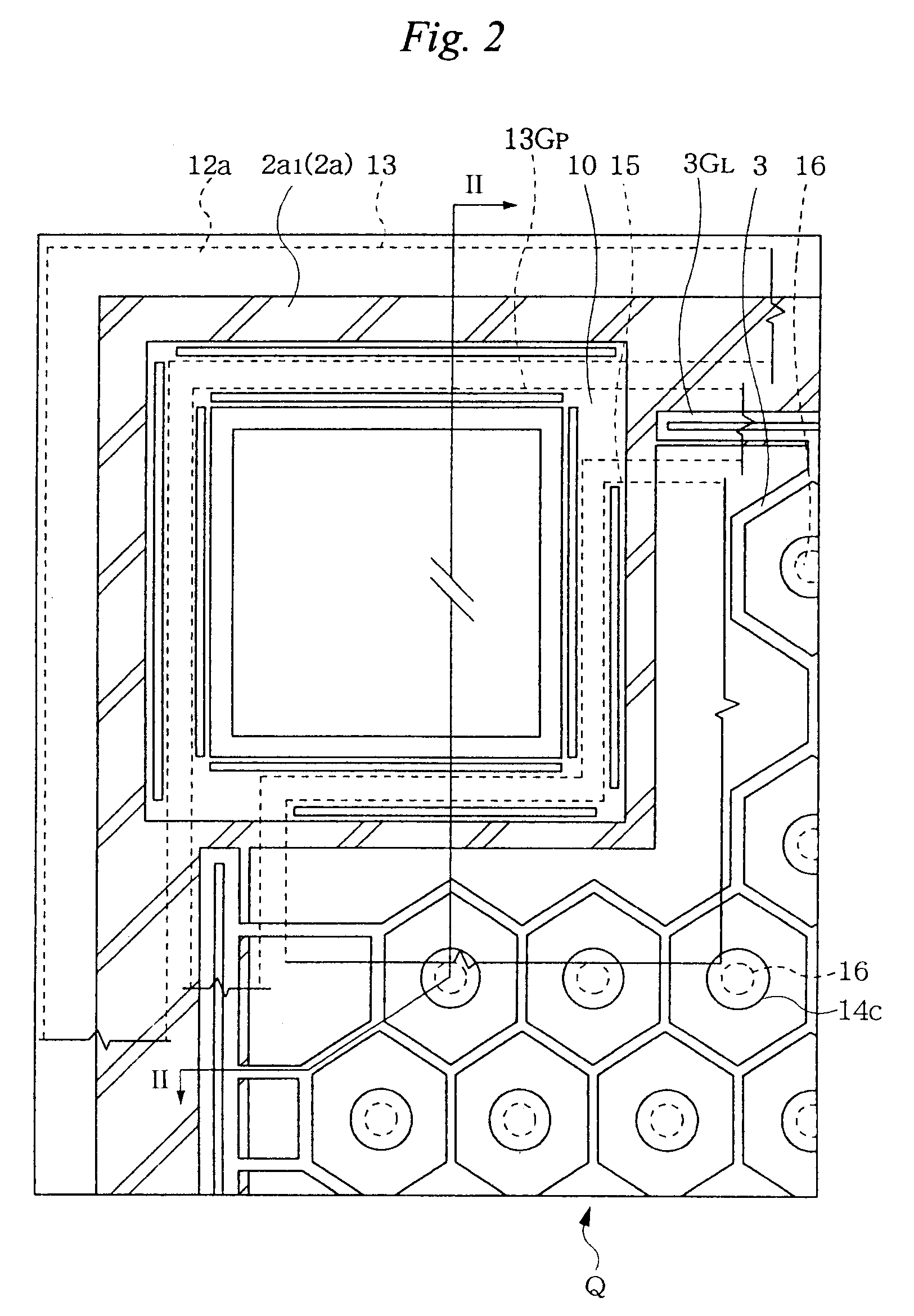
FIG. 1 is a plan view of a semiconductor chip 1 constituting a trench power transistor as the first embodiment of the present invention. FIG. 2 is an enlarged plan view of an area A in FIG. 1. FIG. 3 is a partially sectional view taken in the line B--B of FIG. 2. FIG. 4 is a circuit diagram showing a trench power transistor and an accompanying protective diode.

A semiconductor chip 1 has a semiconductor substrate 1S formed, for example, in a plane rectangular shape. The semiconductor substrate 1S comprises a semiconductor base substance 1SA and an epitaxial layer 1SB formed thereon. The semiconductor base substance 1SA comprises, for example, an n.sup.+ -type silicon single crystal. The epitaxial layer 1SB comprises an n.sup.- -type silicon single crystal formed by, for example, the epitaxial growth. The epitaxial layer 1SB ensures pressure resistance between a source and a drain, and has a resistance value of, for example, approximately 0.25 through 0.36 m.OMEGA.cm...

second embodiment

[Second Embodiment]

The second embodiment describes a modified example of forming the gate insulator and the gate in the trench power transistor. The description in the second embodiment uses the sectional views of the gate formation region in the trench power transistor.

After steps in FIGS. 6 through 8 used for the first embodiment, the semiconductor substrate 1S is cleaned. The second embodiment keeps the opening width of the thick insulator 2b as shown in FIG. 23, namely maintaining the state in FIG. 8. Like the first embodiment, the thermal oxidation treatment is applied to the semiconductor substrate 1S to form the insulator 21 on the trench 7's inner face (side face and bottom face), and then to deposit the oxidation-resistant insulator 22. The semiconductor substrate is is then etched back. As shown in FIG. 24, the oxidation-resistant insulator 22 is left in the trench 7 and on the opening side face of the thick insulator 2b so that the insulator 21 is exposed from the trench ...

third embodiment

[Third Embodiment]

The third embodiment describes another modified example of forming the gate insulator and the gate in the trench power transistor. The description in the third embodiment also uses the sectional views of the gate formation region in the trench power transistor.

Like the first embodiment, the trench 7 is formed on the semiconductor substrate 1S as shown in FIG. 31. The thermal oxidation treatment is then applied to the semiconductor substrate 1S to form the insulator 21 on the trench 7's inner face (side face and bottom face). After the oxidation-resistant insulator 22 is deposited, an etchback process is performed to leave the oxidation-resistant insulator 22 on the trench 7's inner side face and expose the insulator 21 from the trench 7's bottom and the semiconductor substrate 1S's principal plane as shown in FIG. 32. Like the first embodiment, the thermal oxidation treatment is applied to the semiconductor substrate 1S using the oxidation-resistant insulator 22 as...


PUM


Abstract

There are formed a gate insulator 8 and a gate 3 of a power transistor Q having a trench-gate structure. There are then formed a channel region 5 and a source region 6 of the power transistor Q.

Description

TECHNICAL FIELD OF THE INVENTIONThe present invention relates to a semiconductor device manufacturing method and a semiconductor device. Particularly, the present invention relates to a technology that is effectively applicable to a semiconductor device having a trench-gate structured power field-effect transistor (hereafter simply referred to as the trench power transistor).BACKGROUND OF THE INVENTIONThe inventors have examined the following manufacturing technology for trench power transistor. On a principal plane of a semiconductor substrate, there is formed a trench extending in a direction which crosses the principal plane. A gate oxidation treatment is then applied to the semiconductor substrate to form a gate oxidation film on an inner wall face (bottom and side surfaces) of the trench. Subsequently, say a polycrystal silicon film is deposited on the principal plane of the semiconductor substrate by preventing the polycrystal silicon film from filling the trench. Then, a gate...

Claims


Application Information

Patent Timeline
Patent Type & Authority Patents(United States)
IPC IPC(8): H01L29/78H01L21/336H01L21/02H01L29/66H01L29/40H01L29/423H01L29/417
CPCH01L29/7808H01L29/7811H01L29/7813H01L29/41766H01L29/4232H01L29/42368H01L29/4238Y10S438/981
Inventor INAGAWA, HIROSHIMACHIDA, NOBUOOISHI, KENTARO
Owner HITACHI LTD
Why Eureka
Try Eureka