Hetergeneous method for determining module placement in FPGAs

a module placement and heterogeneous method technology, applied in the field of parametric logic modules, can solve the problems of increasing design complexity, designer cannot deal with the entire design at the gate level, and it is difficult to achieve true hierarchical design for fpgas using currently-available softwar

Inactive Publication Date: 2002-09-24
XILINX INC
View PDF45 Cites 102 Cited by
  • Summary
  • Abstract
  • Description
  • Claims
  • Application Information

AI Technical Summary

Benefits of technology

SIMs are easily delivered over a data communications link such as the internet. Therefore, in one embodiment a SIM is protected from duplication or alteration by providing an encrypted SIM that requires a key to decrypt the SIM, using well-known techniques.
In one embodiment, the user can specify a plurality of floorplanners to be applied to different portions of a single FPGA. Where more than one floorplanner is present in a design, the floorplanners may be active simultaneously, and may communicate with each other to implement the SIMs in a fashion that leads to the most desirable overall solution. The most desirable solution is determined by the user, who specifies timing and spatial requirements using known methods such as attaching parameters to a module or setting software options. The ability to run multiple floorplanners simultaneously speeds up the implementation process, due to the parallel processing of the placement task. In other words, this embodiment applies the well-known "divide-and-conquer" strategy to physical layout of an FPGA design.
In one embodiment, the floorplanner can also receive placement information (e.g., from a constraints file or an interactive floorplanner) specifying areas of the target device that are "off limits" to the floorplanner. This ability is useful, for example, when certain portions of a programmable device have been tested and found defective. By specifying and avoiding these defective areas of the device, the rest of the device can still be utilized. The same methods can be used to reserve areas of the target device to be occupied by other modules or elements. Non-SIM elements are easily integrated into a SIM environment using a "black box" interface.

Problems solved by technology

As FPGA designs increase in complexity, they reach a point at which the designer cannot deal with the entire design at the gate level.
True hierarchical design is difficult to achieve for FPGAs using currently-available software.
Designs can be entered hierarchically (e.g., via schematic entry or Hardware Description Languages (HDLs)), but mapping, placement and routing software typically "flattens" the design.
The netlist was encrypted and sent to customers in binary format, which made it difficult to edit or reverse-engineer the netlist.
One disadvantage of the hard macro format was that the area of the FPGA encompassed by the hard macro was totally dedicated to the contents of the macro.
If the logic fit best, or resulted in the fastest performance, in a non-rectangular area, the extra CLBs required to make the area rectangular were wasted.
Therefore, libraries of RPMs are typically large and limited in scope.
The design as a whole can therefore utilize a non-uniform global placement strategy, a technique that is not practical using prior art methods.
While the interconnect fabric of any large FPGA is homogeneous in that it follows a predefined pattern, the interconnect structure typically cannot be segmented into large minimally interacting areas.

Method used


Image

  • Hetergeneous method for determining module placement in FPGAs
  • Hetergeneous method for determining module placement in FPGAs
  • Hetergeneous method for determining module placement in FPGAs

Examples


example sim

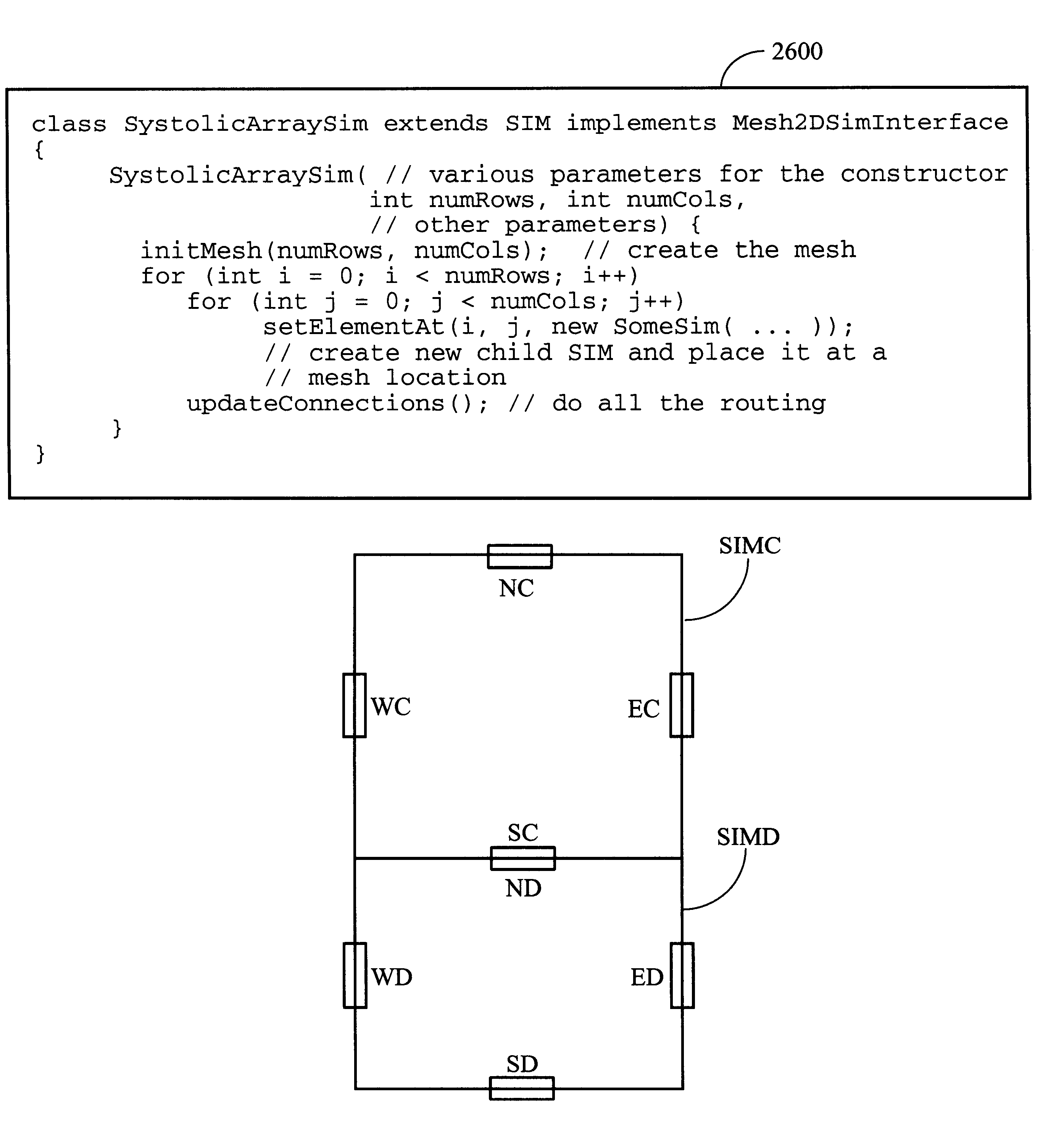
FIG. 2 shows a partial listing 200 of a SIM called X4keAdderxWReg, which illustrates some of the concepts discussed above. In particular, in the example of FIG. 2 it is seen that the width of the adder is established only when an instance of class X4keAdderxWReg is actually instantiated, by calling the constructor of this class. Therefore, the adder implementation is independent of the adder width. The listing shows three ports, "a", "b", and "sum". The listing also shows two internal nets, "cy" and "clsum". One or more instantiations of SIM "CY4" are then added, the number of child SIMs incorporated depending on the "sampleWidth" width parameter set when the adder SIM is instantiated. In this example, CY4 is a carry logic module for Xilinx XC4000 Series FPGAs and is set to functional mode "ADD-FG-CI". Partial listing 200 illustrates static parameter passing as implemented in programming languages such as Java or C. For example, in FIG. 2, the "sampleWidth" parameter is passed from ...

example code 1400

for the PlaceInfo class is shown in FIG. 14. Example code 1400 illustrates a PlaceInfo class including a vector of implementations and methods to enumerate and add these implementations. The PlaceInfo class of FIG. 14 also illustrates including a vector of constraints and methods to enumerate and add these constraints.

FIG. 15 shows exemplary pseudo-code for the Implementation class. (An implementation is represented as an object of the Implementation class.) In an actual Implementation class, the curly braces "{ }" would enclose actual Java code implementing the constructor and the "restore" method. (The comments delimited by the character strings " / **" and "* / " provide information for the JavaDoc utility, which provides on-line documentation for Java code.)

Constraints on a SIM's layout are stored in objects of the Constraint class 1600 shown in FIG. 16. In the example of FIG. 16, a "RegionConstraint" constraint restricts a SIM's layout to be contained in a rectangular device region...

planner examples

FIGS. 18-25 show several examples of Planners using a variety of algorithms.

FIG. 18 shows a Planner 1800 that cycles through a series of precomputed shapes. The SIM designer or user may have created several implementations and stored them in the SIM's PlaceInfo object. The simple Planner in FIG. 18 cycles through all available implementations, scores each implementation according to a predetermined scoring scheme, and selects the implementation with the best score.

FIGS. 19 and 20 show a Planner called "RowPlanner" that is a special-purpose linear Planner. (The Planner comprises the code 1900 of FIG. 19 followed by the code 2000 of FIG. 20.) For a SIM that implements a data path, the constituents are often laid out in a simple linear arrangement. The Planner in FIGS. 19 and 20 performs the layout of such a structure, placing the constituent SIMs in a row. Note that the constituent SIMs need not be identical, nor of the same size. The analogous column Planner ("ColumnPlanner") is very...


PUM


Abstract

The invention provides parametric modules called Self Implementing Modules (SIMs) for use in programmable logic devices such as FPGAS. The invention further provides tools and methods for generating and using SIMs. SIMs implement themselves at the time the design is elaborated, targeting a specified FPGA according to specified parameters. In one embodiment, a SIM references or includes one or more floorplanners each of which may employ one or more placement algorithms. Such placement algorithms might include, for example: a linear ordering algorithm that places datapath logic bitwise in a regular linear pattern; a rectangular mesh algorithm that implements memory in a grid pattern in distributed RAM; a columnar algorithm for counters and other arithmetic logic; or a simulated annealing algorithm for random logic such as control logic. Therefore, a design including more than one SIM can utilize a plurality of placement algorithms at the same or different levels of hierarchy. The design as a whole can therefore utilize a non-uniform global placement strategy.

Description

1. Field of the InventionThe invention relates to programmable integrated circuits (ICs). More particularly, the invention relates to parametric logic modules for implementing designs in programmable ICs, and software tools and methods for creating such modules.2. Description of the Background ArtProgrammable ICs are a well-known type of digital integrated circuit that may be programmed by a user to perform specified logic functions. One type of programmable IC, the field programmable gate array (FPGA), typically includes an array of configurable logic blocks (CLBs) surrounded by a ring of programmable input / output blocks (IOBs). The CLBs and IOBs are interconnected by a programmable interconnect structure. The CLBs, IOBs, and interconnect structure are typically programmed by loading a stream of configuration data (bitstream) into internal configuration memory cells that define how the CLBs, IOBs, and interconnect structure are configured. The configuration data may be read from me...

Claims


Application Information

Patent Timeline
Patent Type & Authority Patents(United States)
IPC IPC(8): G06F17/50
CPCG06F17/5072G06F30/392
Inventor HWANG, L. JAMESDELLINGER, ERIC F.MITRA, SUJOYMOHAN, SUNDARARAJARAOPATTERSON, CAMERON D.WITTIG, RALPH D.
Owner XILINX INC
Why Eureka
Try Eureka