Method and apparatus to manufacture an electronic package with direct wiring pattern

a technology of electronic assembly and wiring pattern, applied in the direction of final product manufacturing, sustainable manufacturing/processing, coupling device connection, etc., can solve the problems of increasing production cost, increasing mechanical stress level of assembly, and reducing product reliability, so as to reduce production cost and reduce size

Inactive Publication Date: 2002-10-01
IBM CORP
View PDF12 Cites 118 Cited by
  • Summary
  • Abstract
  • Description
  • Claims
  • Application Information

AI Technical Summary

Benefits of technology

Another object of the invention is to provide an improved electronic assembly package having decreased size.
It is yet another object of the present invention to provide an improved electronic assembly package which decreases production costs at the first and / or second level attachment.
Still another object of the invention is to provide a method of making and assembling an improved electronic assembly package having enhanced yield and reliability.

Problems solved by technology

However, even with such attachment means, a large CTE mismatch can still cause failure at various sites in the attachment when the first level packaging is made from a ceramic or metal composite.
When the first level package Coefficient of Thermal Expansion (CTE) is different than the CTE of the second level package, any increase in the size of the first level package size will result in an increased mechanical stress level of the assembly, consequently resulting in decreased product reliability.
The above methods of attaching two electronic modules having differing array size, shape, pitch, and the like, with increased I / O count, leads to increased production costs, increased size of the resulting second level attachment, and decreased reliability.

Method used


Image

  • Method and apparatus to manufacture an electronic package with direct wiring pattern
  • Method and apparatus to manufacture an electronic package with direct wiring pattern
  • Method and apparatus to manufacture an electronic package with direct wiring pattern

Examples


Embodiment Construction

)

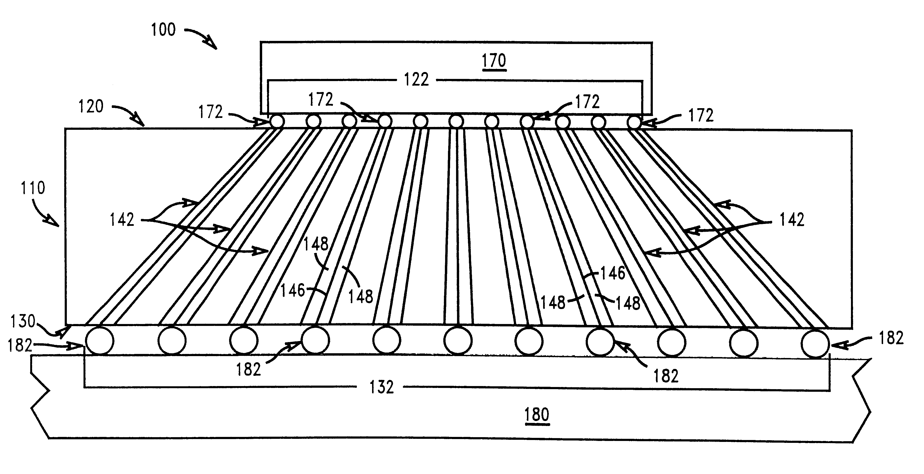
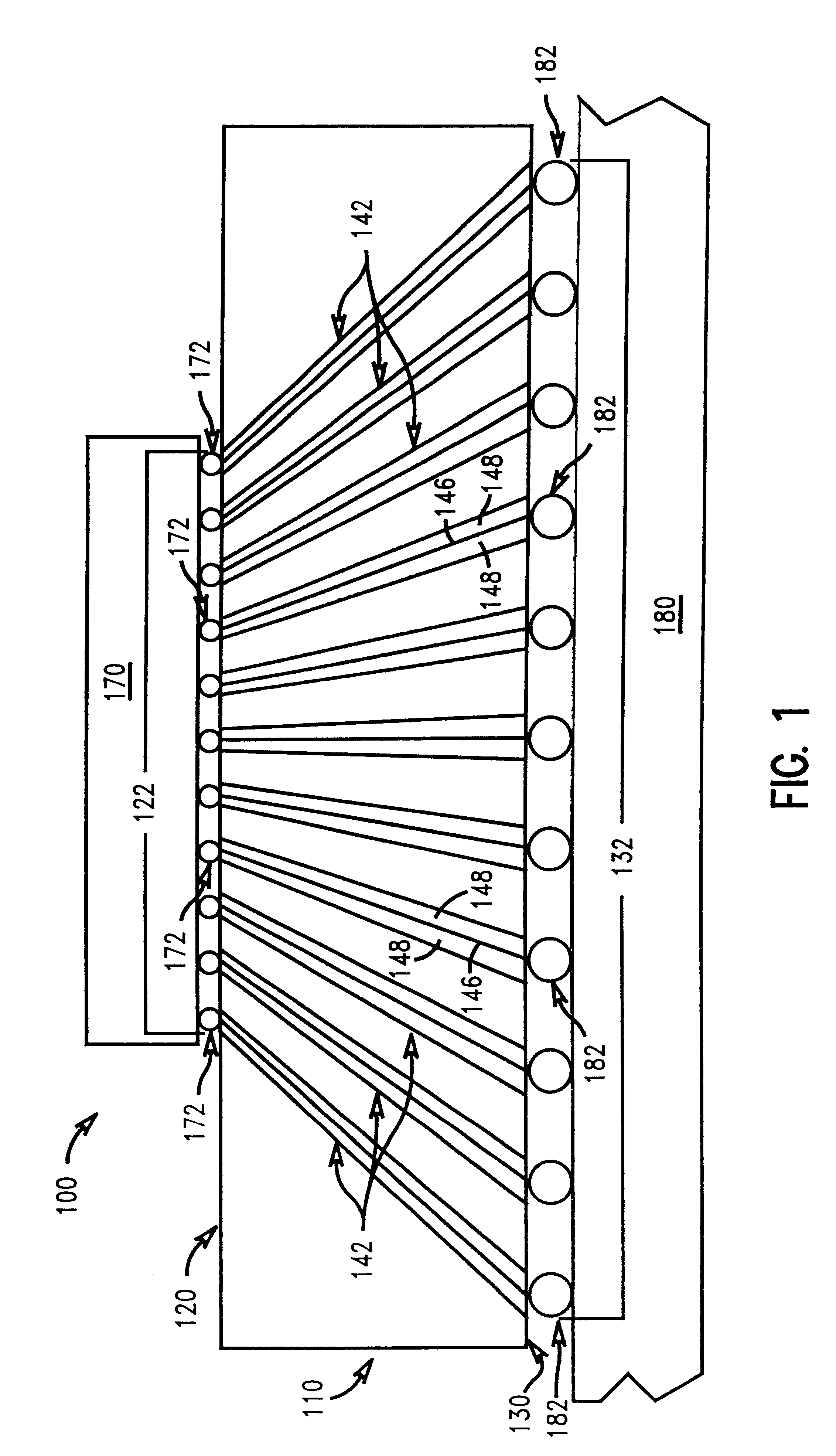
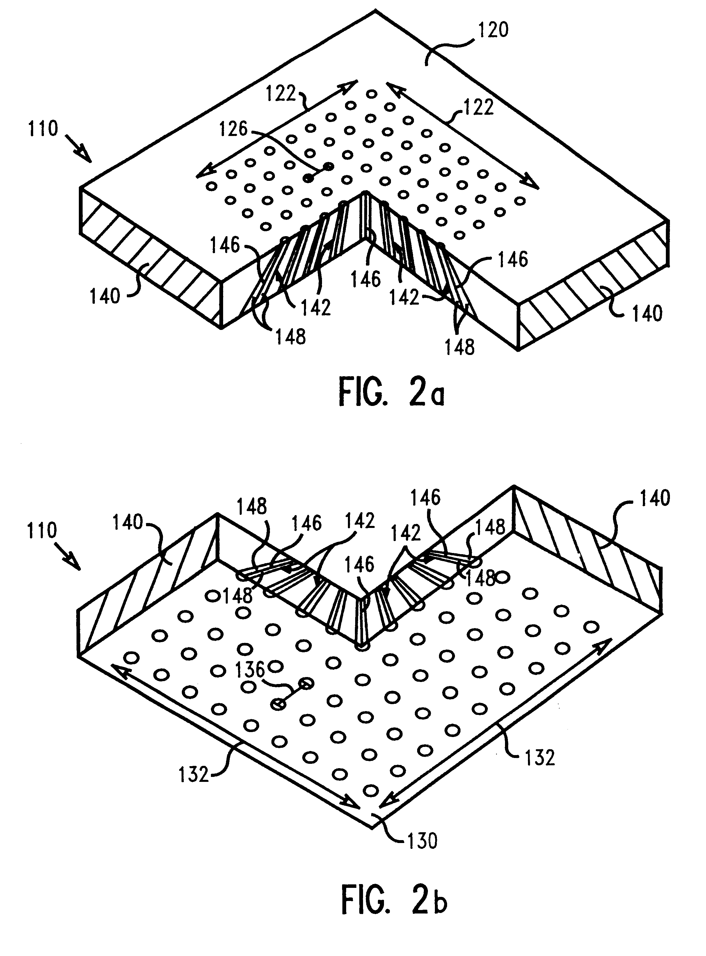
In describing the preferred embodiment of the present invention, reference will be made herein to FIGS. 1-5D of the drawings in which like numerals refer to like features of the invention. Features of the invention are not necessarily shown to scale in the drawings. Numerous embodiments of the present invention are possible, including the embodiments described below.

The present invention comprises an electronic package assembly and a method of making the same which provides an electrical interconnection between two electronic modules having the same number of I / O arrays but differing conductive array parameters. Such conductive array parameters are defined as I / O array pitch, size, shape, type of array, such as conductive leads, pins, wires, pads, balls, fingers, and any other mating system known in the art, and combinations thereof. Such electronic module interconnections include, for example, an IC package to a circuit board, wherein the IC package may comprise a SCM, MCM, or an ...


PUM


Abstract

An electronic package assembly for electrical interconnection between two electronic modules having differing conductive array parameters is disclosed. The electronic package assembly includes two electronic modules, providing between the two electronic modules an interposer having a top surface and a bottom surface; a first set of conductive arrays having a first conductive array parameter on the top surface, and a second set of conductive arrays having a second conductive array parameter on the bottom surface, the second conductive array and the first conductive array having differing parameters. A plurality of conductors traverses a thickness of the interposer of the electronic package assembly, with the conductors including a conductive material optionally coated with a dielectric material, the conductors having a first end at the first conductive arrays and a second end at the second conductive arrays, whereby the conductors connecting the first and second conductive arrays therein are adapted to spatially transform the differing parameters to provide an electrical interconnection. A conductive matrix surrounds the conductors of the interposer of the electronic package assembly. The first set of conductive arrays includes the same conductive array parameters as a first electronic module and the second set of conductive arrays includes the same conductive array parameters as a second electronic module.

Description

1. Field of the InventionThe present invention relates to electronic assembly packages, and in particular, to an apparatus and method of making an electronic assembly package wherein two electronic modules, having differing conductive array parameters, are electrically and mechanically interconnected by an interposer structure which spatially transforms such differing conductive array parameters thereby forming the electronic assembly package.2. Description of Related ArtIn surface mount technology, integrated circuits (ICs) have leads, or signal Input / Output (I / O) connections, and Power / Ground (P / G) connections which are connected to ceramic or organic packages which in turn also have leads extending therefrom. Such IC assemblies include, for example, single chip modules (SCM), wherein one chip is connected to a single chip module, or multi-chip module (MCM), wherein more than one chip is connected to an organic or ceramic package containing multi-layers of thick-film or thin-film...

Claims


Application Information

Patent Timeline
Patent Type & Authority Patents(United States)
IPC IPC(8): H01L23/48H01L23/498H05K3/34H05K1/11
CPCH01L23/49827H05K3/3436H01L2224/16H01L2924/01079H01L2924/15174H01L2924/15311H01L2924/3011H05K1/113H05K2201/09836H05K2201/10378H01L2924/00014Y02P70/50H01L23/49816H01L23/15H01L2224/0401
Inventor BEZAMA, RASCHID J.NATARAJAN, GOVINDARAJANPASCO, ROBERT W.
Owner IBM CORP
Why Eureka
Try Eureka