Double planar gated SOI MOSFET structure

a semiconductor field effect transistor and double-planar gate technology, applied in the direction of transistors, semiconductor devices, electrical equipment, etc., can solve the problems of poor quality and/or more poorly controlled devices, slow device performance, and difficult fabrication of such structures

Inactive Publication Date: 2002-11-19
GLOBALFOUNDRIES INC
View PDF16 Cites 220 Cited by
  • Summary
  • Abstract
  • Description
  • Claims
  • Application Information

AI Technical Summary

Problems solved by technology

The fabrication of such structures is difficult because the top and bottom gates must be aligned to a tolerance beyond the accuracy of state of the art lithographical equipment and methods, and because self-aligning techniques are frustrated by the layers between the top and bottom gates.
However, the alignment of the top and the bottom is crucial to high performance because a mis-alignment will cause extra gate to source / drain overlap capacitance as well as loss of current drive.
However, the double-gate MOSFET with a planar structure either does not have perfectly aligned gates, or did not have a source / drain fan-out structure that is self-aligned to the gates.
The key difficulties in fabricating double-gated FETs are achieving silicidation of thin diffusions or polysilicon with acceptable contact resistance, enabling fabrication of the wraparound gate without misalignment of the two gates, and fabrication of the narrow diffusions (ideally, 2-4 times smaller than the gate length).
First, definition of the gate may leave poly spacers on the side of the diffusions or may drive a required slope on the side of the diffusion, thereby resulting in a poorer quality and / or more poorly controlled device.
Second, the slope of the poly inherently leads to difficulty in forming silicided gates, leading to slower device performance.
Finally, the poly step height poses a difficult problem for lithographic definition, as we expect steps on the order of 100 nm-200 nm in a 50 nm design rule technology.

Method used


Image

  • Double planar gated SOI MOSFET structure
  • Double planar gated SOI MOSFET structure
  • Double planar gated SOI MOSFET structure

Examples


second embodiment

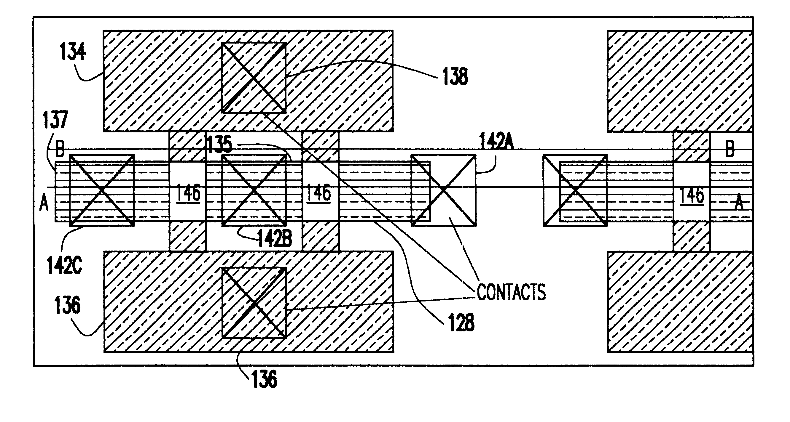
A second embodiment is shown in FIGS. 12, 13A and 13B. In FIG. 12, a dielectric pad films 118, 120 and 122 electrically separate the gate 130 into two electrically isolated portions 135, 137. As shown in FIG. 13B, each portion 135, 137 has a planar top surface and a contact 142a, 142b, 142c on its respective planar top surface. The gate 128 is independently controlled on each side of the diffusion. However, a linear strap of metal, or a patterned layer to link the layers with a silicide can also be utilized. Note that in FIG. 13B the fingered devices become larger because etch stretch of polysilicon would have to be individually contacted unless additional masking layers are used to strap them together.

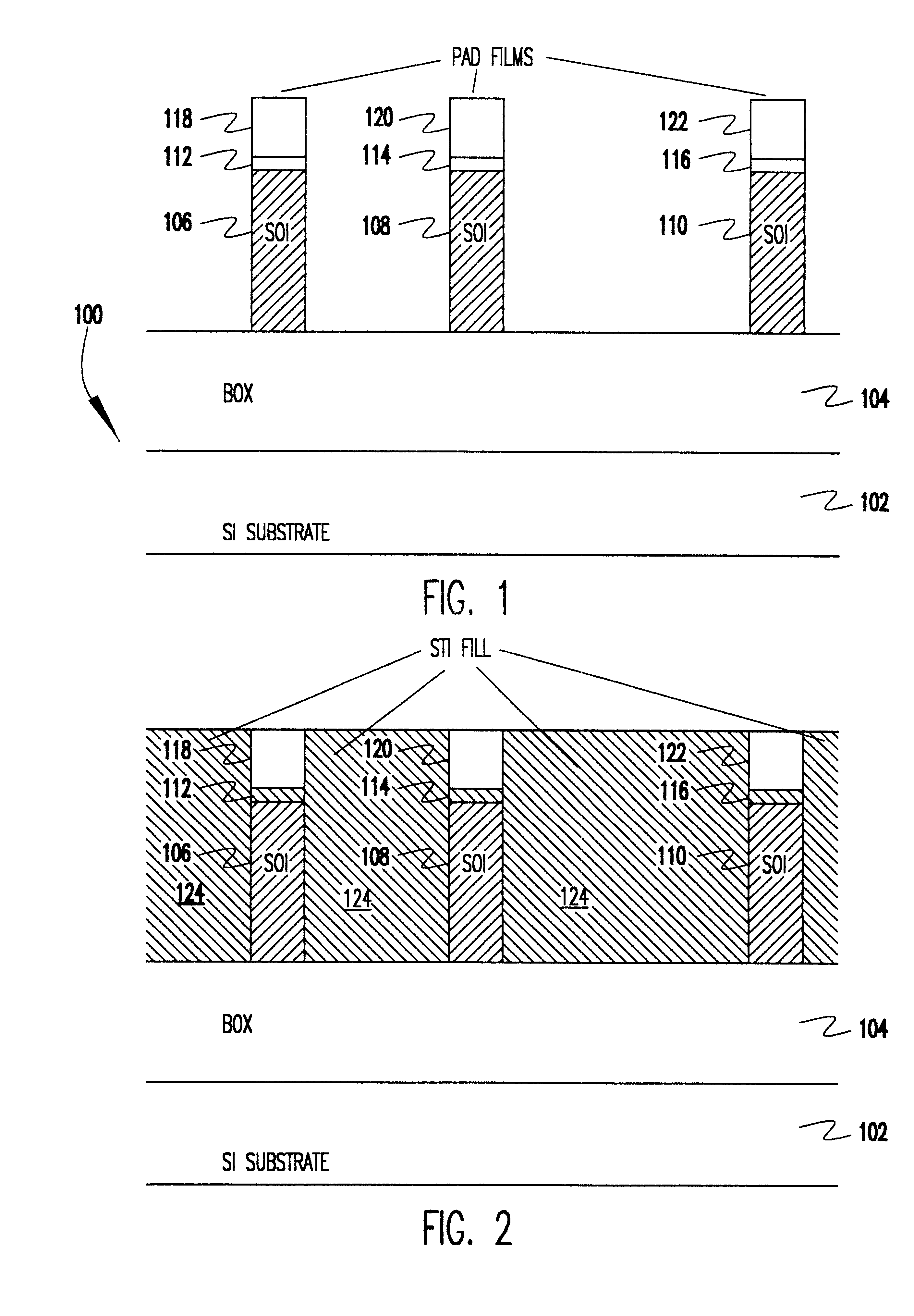
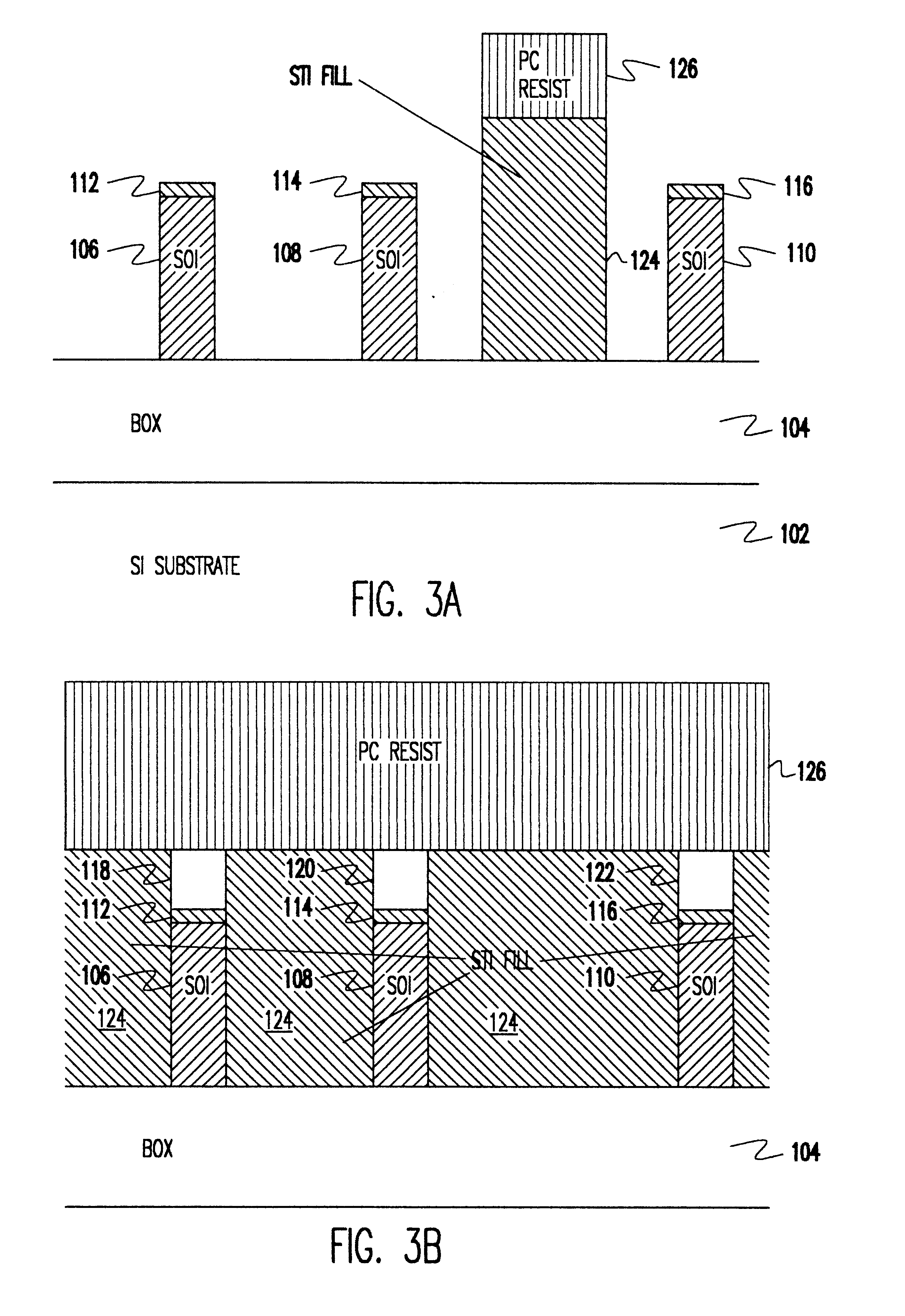
In the second embodiment, the processing steps are identical to those described up to and including FIG. 2. However, in FIG. 12, as opposed to FIG. 3A, pad films 118, 120, 122 are not etched. In this embodiment, it is preferred that the pad films be 80-150 nm.

FIG. 13A, corresponding t...

fifth embodiment

The fifth embodiment continues from the previous embodiments, but the fourth embodiment will be used as the base. After the gate 128 is formed as above by deposition, polishing and etching, the device implants are completed, spacers 146 are formed and the diffusions are annealed, a layer of highly conformal dielectric fill 148 is deposited, and then polished to the top of the gate conductor. Note that in this case it is preferable to deposit a polish-stop layer 150 (typically a dielectric such as silicon nitride) as a cap on top of the original dummy gate conductor 152 after it has been polished but before it has been etched. Fabrication of this structure is shown in cross section in FIG. 19.

This dummy gate cap layer 150 and the dummy gate conductor 152 are then removed, a gate dielectric deposited and a second gate conductor deposited. This approach is advantageous if either the gate conductor or gate dielectric cannot withstand the high temperature steps required in forming the di...


PUM


Abstract

A double gated silicon-on-insulator (SOI) MOSFET is fabricated by using a mandrel shallow trench isolation formation process, followed by a damascene gate. The double gated MOSFET features narrow diffusion lines defined sublithographically or lithographically and shrunk, damascene process defined by an STI-like mandrel process. The double gated SOI MOSFET increases current drive per layout width and provides low out conductance.

Description

1. Field of the InventionThe present invention generally relates to double-gated Silicon-on-Insulator (SOI) Metal Oxide Semiconductor Field Effect Transistors (MOSFETs) that provide increased current drive per layout width and low output conductance.2. Background DescriptionField Effect Transistor (FET) structures may include a single gate (a single channel) or a pair of gates (a pair of channels), with double-gate versions providing the advantage of having an increased current carrying capacity. A number of horizontal double-gate FET structures, and particularly SOI double-gate FET structures, have been proposed. These structures typically require a bottom gate formed beneath the thin silicon body in addition to a conventional top gate. The fabrication of such structures is difficult because the top and bottom gates must be aligned to a tolerance beyond the accuracy of state of the art lithographical equipment and methods, and because self-aligning techniques are frustrated by the ...

Claims


Application Information

Patent Timeline
Patent Type & Authority Patents(United States)
IPC IPC(8): H01L21/336H01L21/02H01L29/786H01L27/12H01L21/762H01L21/70H01L21/84H01L29/66
CPCH01L21/76264H01L21/84H01L27/1203H01L29/66545H01L29/66795H01L29/785H01L21/76283
Inventor ADKISSON, JAMES W.BRACCHITTA, JOHN A.ELLIS-MONAGHAN, JOHN J.LASKY, JEROME B.LEOBANDUNG, EFFENDIPETERSON, KIRK D.RANKIN, JED H.
Owner GLOBALFOUNDRIES INC
Why Eureka
Try Eureka