Stackable semiconductor device and method for manufacturing the same

a semiconductor device and chip technology, applied in the direction of manufacturing tools, electrical apparatus construction details, printed circuit non-printed electric components association, etc., can solve the problem of limiting the miniaturization of electronic parts, difficult to form solder ball bumps with even heights in one ic chip, and increasing the mounting density of parts

Inactive Publication Date: 2003-01-07
SONY CORP
View PDF12 Cites 106 Cited by
  • Summary
  • Abstract
  • Description
  • Claims
  • Application Information

AI Technical Summary

Problems solved by technology

To realize the size reduction, thinning, and weight reduction of the portable equipment, the increase in part mounting density is an important problem.
According to this method, there is a problem that since the thickness of solder deposited by electrolytic plating is affected by the state of the surface of a primary material layer and slight fluctuation of electric resistance, it is fundamentally difficult to form solder ball bumps with even heights in one IC chip.
However, in consideration of only two-dimensional space, there is a limit on miniaturization of electronic parts, and so a mounting space must be designed from the viewpoint of not only two-dimensional direction, but also three-dimensional direction.
In other words, if there is a flaw on the back of the wafer W, the strength of the flaw portion is decreased and there is a danger that breakage of the wafer begins from the flaw portion.
However, removing damages such as flaws on the back of the wafer increases the strength of the wafer W even if it is thinned.

Method used


Image

  • Stackable semiconductor device and method for manufacturing the same
  • Stackable semiconductor device and method for manufacturing the same
  • Stackable semiconductor device and method for manufacturing the same

Examples


Embodiment Construction

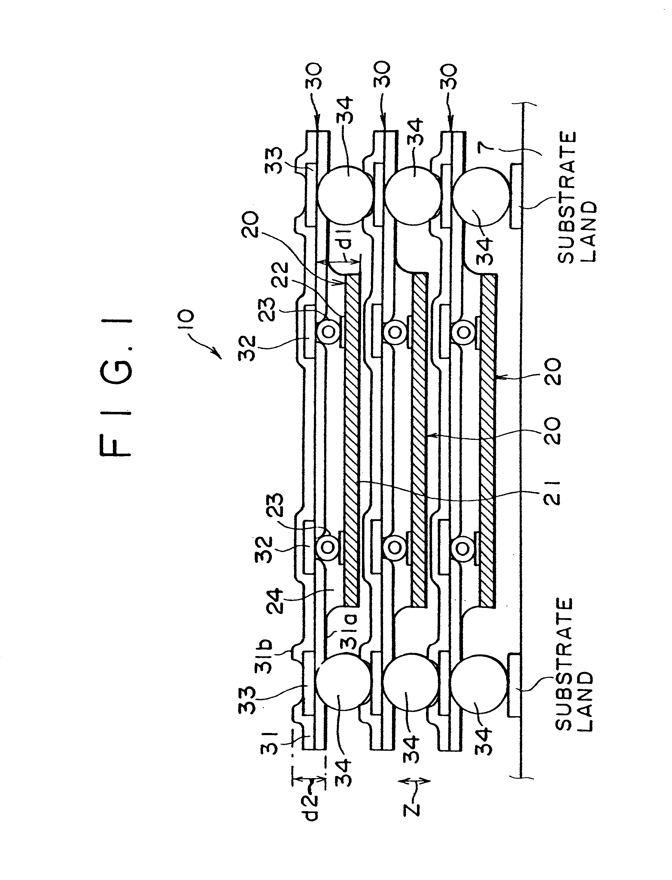
FIGS. 6 to 8 shows another preferred embodiment of the method for manufacturing a semiconductor device of the present invention.

First, in FIG. 6A, almost spherical third protrusion electrodes 23a using high-melting solder are formed in the place redisposed with a BLM film from electrode pad 25 around respective semiconductor chips 20 of the wafer W. The inner bump 23 is formed on the BLM film 27 exposed from the opening section 28a of a polyimide film 28.

Next, as shown in FIG. 6B, after liquid resin 24 such as epoxy resin or suchlike is applied to the whole surface of the wafer in a manner of spin coating, the liquid resin 24 is hardened by thermal treatment of curing at approx. 150.degree. C. for about five hours.

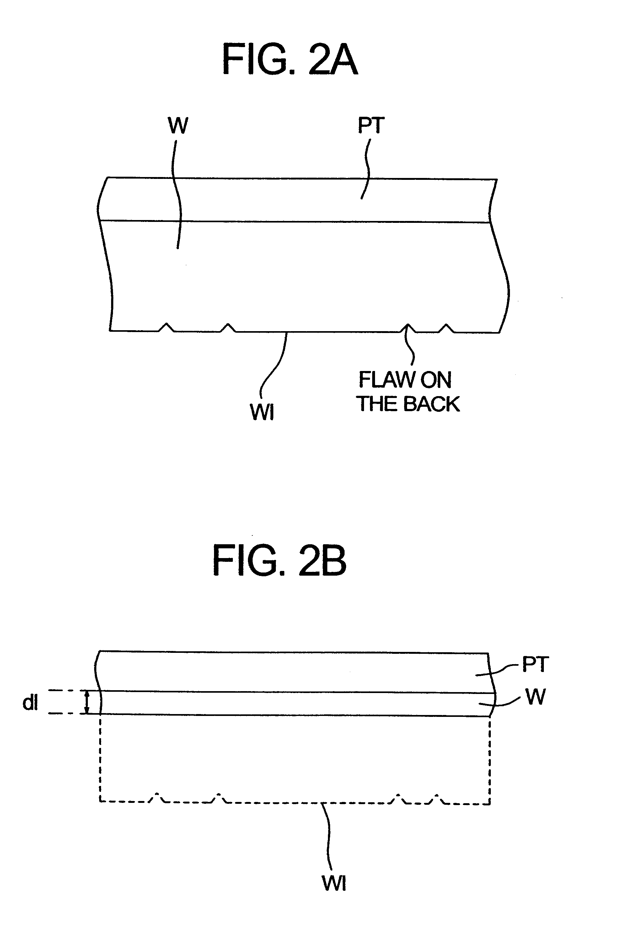
Further, a protective tape PT is pasted on the surface of the wafer W where the third protrusion electrodes 23a are formed, and the back of the wafer W is ground by means of the grinding machine shown in FIG. 3. At this time, the grinding is performed at the feed speed of ...


PUM

PropertyMeasurementUnit
thicknessaaaaaaaaaa
thickness d1aaaaaaaaaa
thickness d2aaaaaaaaaa

Abstract

There is provided a semiconductor device having a semiconductor chip in which a first protrusion electrode is formed on the semiconductor substrate; and an intermediate substrate which comprises a base substrate, a first external terminal provided in said base substrate, which is joined to said first protrusion electrode, a second external terminal provided in said base substrate, an electrode section being exposed on both surfaces of said base substrate, and a second protrusion electrode formed at one end face of said second external terminal, a plurality of said intermediate substrates being stacked in layers by joining said second protrusion electrode to the other end face of said second external terminal, thus enabling miniaturizing and lightening electronic equipment and realizing high reliability and high performance.

Description

RELATED APPLICATION DATAThe present application claims priority to Japanese Application No. P10-294155 filed Oct. 15, 1998; Japanese Application No. P10-311057 filed Oct. 30, 1998 and Japanese Application No. P10-371006 filed Dec. 25, 1998 which applications are incorporated herein by reference to the extent permitted by law.1. Field of the InventionThe present invention relates to the method for manufacturing a semiconductor device and retrofitting of a semiconductor device and more particularly to a semiconductor manufacturing method and a semiconductor device based on the structure of a semiconductor substrate disposed on a printed wiring board (PWB).2. Description of the Related ArtDigital video cameras, digital portable telephones, and portable electronic equipment such as notebook type personal computers has recently been widely popular and this has increased the need for smaller, thinner, and more lightweight portable equipment.To realize the size reduction, thinning, and wei...

Claims


Application Information

Patent Timeline
Patent Type & Authority Patents(United States)
IPC IPC(8): H01L25/065H01L23/12
CPCH01L25/0657H01L2224/1147H01L2924/10253H01L2224/73204H01L2224/32225H01L2224/16225H01L2924/01322H01L2224/16237H01L2225/06517H01L2225/0652H01L2225/06541H01L2225/06572H01L2225/06586H01L2924/09701H01L2924/1532H01L2924/15331H01L2924/00012H01L2924/00H01L24/05H01L2224/02377H01L2224/05001H01L2224/05022H01L2224/05024H01L2224/05548H01L2224/05572H01L23/12
Inventor YANAGIDA, TOSHIHARU
Owner SONY CORP
Why Eureka
Try Eureka