

Microwave transistor subjected to burn-in testing
- Summary
- Abstract
- Description
- Claims
- Application Information
AI Technical Summary
Benefits of technology
Problems solved by technology
Method used
Image

Examples
first embodiment
the present invention will now be described below with reference to FIGS. 1 to 5.
According to this embodiment, an internally matched GaAs FET operating at 18 GHz in class A or class AB operation (having a matching circuit for 18 GHz incorporated in the package) is burned in.
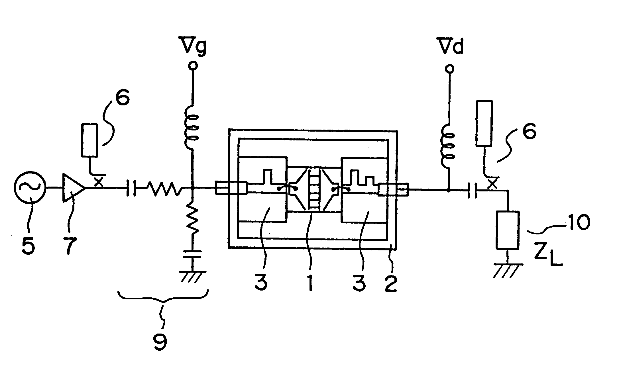
FIG. 1 is a schematic diagram showing one channel portion of a burn-in apparatus which bums in a device having an operating frequency of 18 GHz at a burn-in frequency of 800 MHz. In the drawing, reference numerals identical with those used in FIG. 14 denote the same or corresponding portions. Numeral 10 denotes a resistive load, 9 denotes an input side low-frequency matching circuit and 10 denotes an output side low-frequency matching circuit.
In FIG. 1, the semiconductor device to be burned in is an internally matched FET as described above, and therefore a matching circuit 3 for 18 GHz is incorporated in the package 2. However, at a low frequency such as 800 MHz, parasitic capacitance and inductance of the match...
embodiment 2
A second embodiment of the present invention will now be described below with reference to FIGS. 5 to 10.
In contrast to the first embodiment wherein an FET used in class A operation is burned in, this embodiment refers to a burn-in process of internally matched GaAs FET used in class C or class F operation at a frequency of 18 GHz.
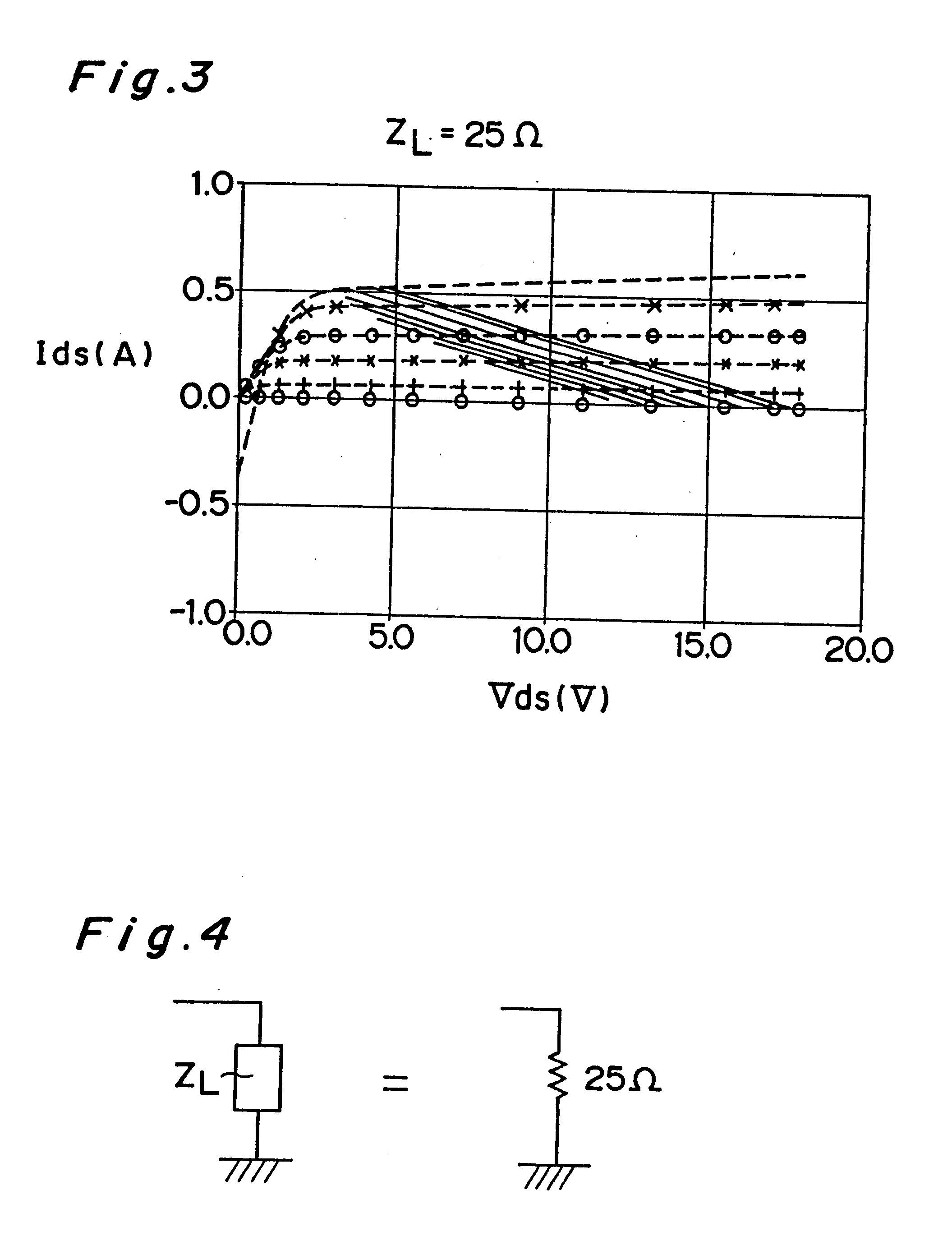
While class B or class F operation is employed in order to achieve high-efficiency transistor operation, a sufficient load cannot be applied to the FET by simply using 1 S a resistor for the load 10, as in the first embodiment. For the transistor used for such a high-efficiency class of operation, it is necessary to take into consideration the effect of harmonics being generated.
FIG. 5 shows a load (Z,) which is matched for high frequency for use in burn-in of an FET designed for class B operation in this embodiment. In the drawing, L and C are parameters which cause resonance at the burn-in frequency (800 MHz), namely that satisfy the relationship 2.pi.f=...
embodiment 3
A third embodiment of the present invention will now be described below with reference to FIGS. 11 and 12.
While the first and the second embodiments relate to the burn-in process of an internally matched GaAs FET used in class A, class C, or class F operation, there are others which show complicated load curves as shown in FIG. 11.
In order to burn in such an internally matched GaAs FET, there is a method of low-frequency burn-in at 800 MHz, wherein substantially the same electrical stress as that of the operating frequency, 18 GHz, is applied to the transistor by using a virtual load having a characteristic curve that passes through the points (Id1, Vd1), (Id2 , Vd2), and (Id3, Vd3) of FIG. 11.
When such a method is used, burn-in effect similar to that obtained under the conditions of FIG. 11 can be achieved by using a combination of R, L, and C for the load (ZL) 10 of the burn-in apparatus shown in FIG. 1. An imaginary load curve determined by the combination passes key points (a po...
PUM
 Abstract
Description
Claims
Application Information