Appearance inspection machine and method for concurrently performing defect detection and classification

a technology of appearance inspection machine and classification method, which is applied in the direction of image enhancement, semiconductor/solid-state device testing/measurement, instruments, etc., can solve the problems of accumulating defects at one step, enormous number of defects would be found at the last step, and inability to meet cost and labor, so as to shorten the processing time and improve the throughput of inspection

Inactive Publication Date: 2003-02-11
TOKYO SEIMITSU
View PDF9 Cites 98 Cited by
  • Summary
  • Abstract
  • Description
  • Claims
  • Application Information

AI Technical Summary

Benefits of technology

The present invention attempts to solve the foregoing problems. An object of the present invention is to provide an appearance inspection machine and method capable of classifying a defect automatically and efficiently and analyzing a defect for a short time. Specifically, the present invention is intended to shorten the processing time required for an entire appearance inspection and to improve the throughput of inspection.
Conventionally, since the time required for automatically defect classification is insufficient, a significant defect is mainly analyzed. Image comparison is achieved by judging whether a difference between two image data items is larger than a set value. However, according to the present invention, automatic defect classification can be achieved accountely. During image comparison, information concerning the location and size of a defective part, the gray-scale level thereof, and a difference in gray-scale level thereof from a compared part can be output as defect information. An amount of image data to be checked for selecting an analysis-needed part, that is, for automatically classifying a defect is adjusted dynamically according to an amount of image data that can be checked for automatically classifying a defect within a certain time. For example, the occurrence frequency of a defect is low for some time since the start of inspection. The occurrence frequency may rise in the course of inspection. In this case, the criterion of selecting an analysis-needed part is lowered so that even a small defect will be selected as an analysis-needed part. In the course of inspection, the criterion of selection is raised so that the small defect will not be selected as an analysis-needed part. Consequently, an ADC system can be operated efficiently.
The storage capacity of the analysis buffer memory depends on the processing time required until an analysis-needed part is selected, and must be large enough to store image data acquired by scanning a row having the largest number of dice. In this case, the analysis buffer memory can be controlled easily.

Problems solved by technology

If a defect occurred at each step, an enormous number of defects would be found at the last step.
This is because a defect occurring at one step is accumulated on defects having occurred previously.
However, this is unfeasible in terms of cost and labor.
The processing time is therefore very long.
The time that can be spent for inspecting the appearance of one semiconductor wafer is limited and must be further shortened.
This brings about the current situation that analysis cannot be carried out satisfactorily.

Method used


Image

  • Appearance inspection machine and method for concurrently performing defect detection and classification
  • Appearance inspection machine and method for concurrently performing defect detection and classification
  • Appearance inspection machine and method for concurrently performing defect detection and classification

Examples


Embodiment Construction

Before proceeding to a detailed description of the preferred embodiments, a prior art will be described with reference to the accompanying relating thereto for a clearer understanding of the differences between the prior art and the present invention.

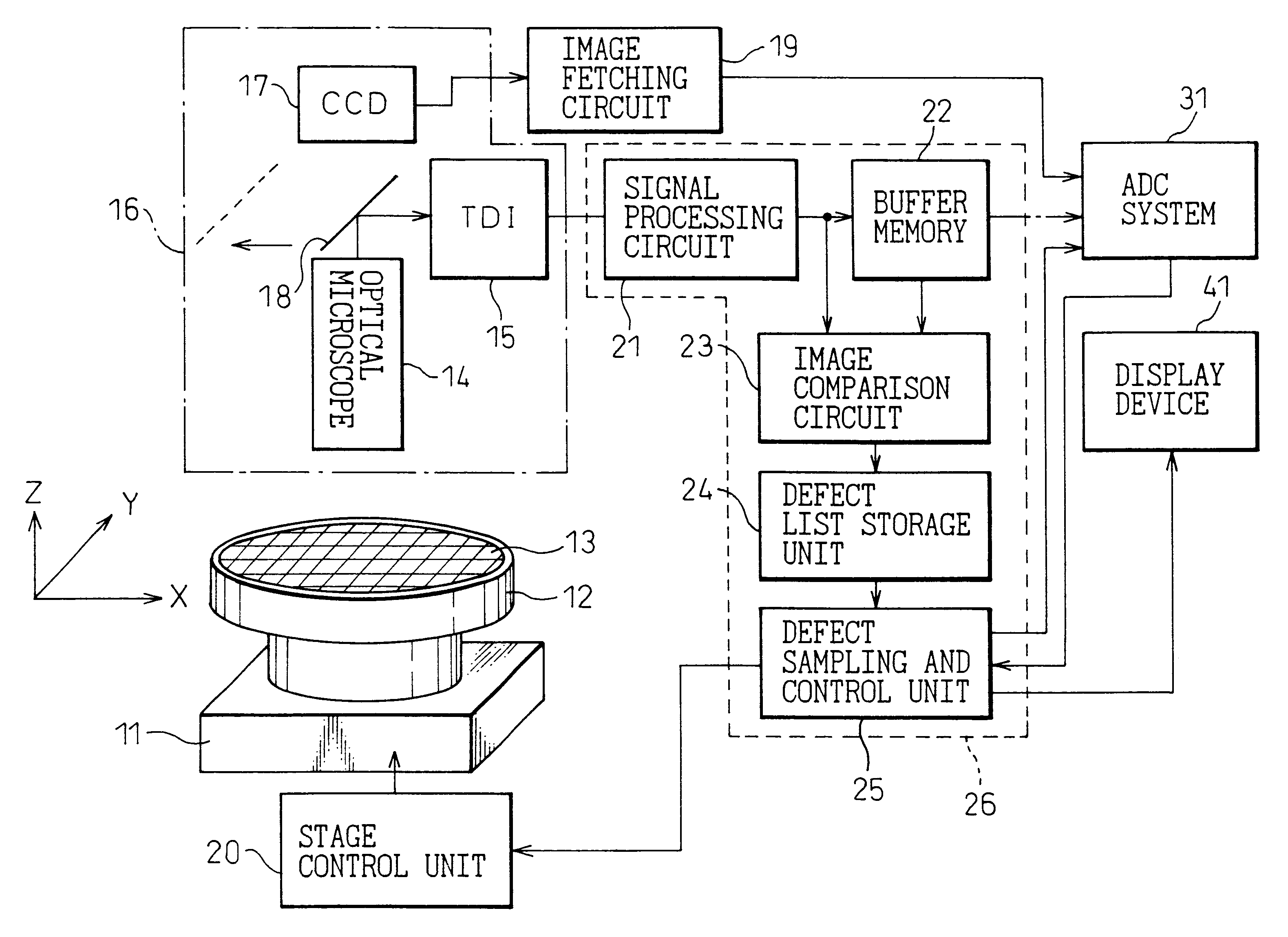
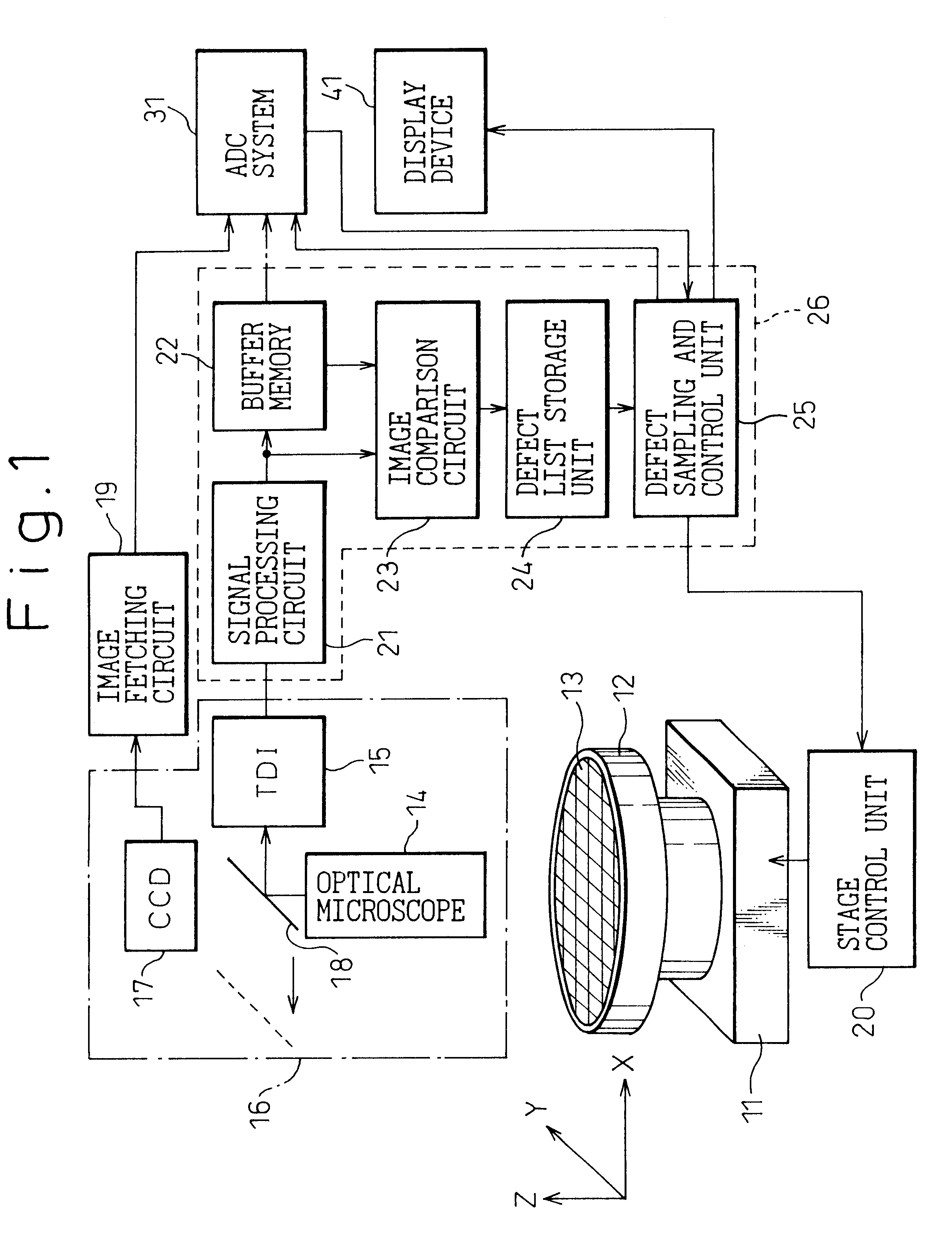
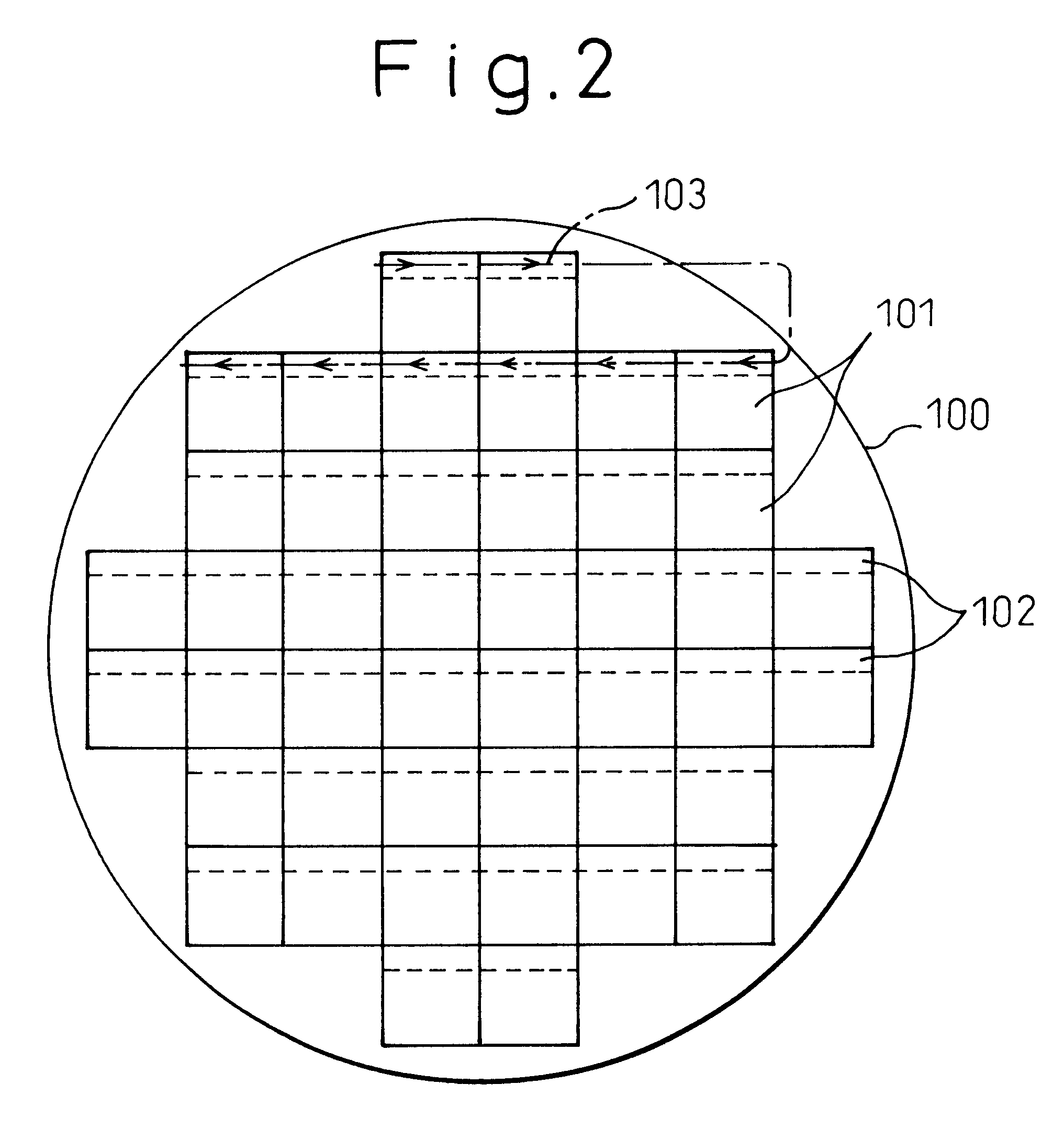
FIG. 1 shows an appearance inspection machine for semiconductor wafers in accordance with a prior art. FIG. 2 shows a trajectory according to which a semiconductor wafer is scanned to acquire image data during inspection. FIG. 3 and FIG. 4 are flowcharts describing appearance inspection in accordance with the prior art.

As shown in FIG. 1, an appearance inspection machine of a prior art has a semiconductor wafer 13, which has a plurality of dice (chips) formed thereon, mounted on a sample holder 12 installed on a stage 11. The stage 11 has movements thereof controlled by a stage control unit 20. An optical microscope 14 magnifies and projects an image depicting the surface of the semiconductor wafer 13. In the prior art, either of a TDI ...


PUM

PropertyMeasurementUnit
defectaaaaaaaaaa
sizeaaaaaaaaaa
areaaaaaaaaaaa

Abstract

Disclosed is an appearance inspection machine comprising an image acquisition unit, a defect information production unit, and an automatic defect classification unit. The defect information production unit detects a defect by comparing two image data and produces defect information. The automatic defect classification unit autonomously classifies a defect according to image data of a defective part concerned. The defect information production unit consists of a comparison buffer memory, an image comparison unit, an analysis buffer memory, and a sampling and control unit. Image data is temporarily stored in the comparison buffer memory. The image comparison unit detects a defect by comparing image data of one die with image data of other two dice. Image data is temporarily stored in the analysis buffer memory. The sampling and control unit selects an analysis-needed part according to defect information and transfers necessary image data to the automatic defect classification unit. As soon as defect information is produced, the sampling and control unit selects an analysis-needed part and transfers necessary image data. Thus, defect detection and classification are partly carried out concurrently.

Description

BACKGROUND OF THE INVENTION1. Field of the InventionThe present invention relates to an appearance inspection machine and method for semiconductor wafers. More particularly, this invention is concerned with a technology for quickly inspecting the appearance of a semiconductor wafer as a whole.2. Description of the Related ArtIn general, a semiconductor wafer manufacturing process consists of about 300 to 500 steps. If a defect occurred at each step, an enormous number of defects would be found at the last step. This is because a defect occurring at one step is accumulated on defects having occurred previously. For improving the yield of a product, ideally, the appearance of the product is inspected at each step. However, this is unfeasible in terms of cost and labor. In reality, the appearance of the product is inspected at some steps. For further improving the manufacturing efficiency, appearance inspection should preferably be included in the manufacturing process. There is theref...

Claims


Application Information

Patent Timeline
Patent Type & Authority Patents(United States)
IPC IPC(8): G06T7/00G01N21/93G01N21/88G01N21/956G06T1/00H01L21/66
CPCG06T7/001G06T2207/30144
Inventor TAKEUCHI, NAOYA
Owner TOKYO SEIMITSU
Why Eureka
Try Eureka