System and method for estimating capacitance of wires based on congestion information

a technology of congestion information and system and method, applied in pulse technique, semiconductor/solid-state device testing/measurement, instruments, etc., can solve the problems of over-estimation of capacitance, difficulty in computing the capacitance of wires based on the steiner tree topology, and improper connection or placement of physical items within one or more cells by the designer

Inactive Publication Date: 2003-02-11
MAGMA DESIGN AUTOMATION
View PDF3 Cites 37 Cited by
  • Summary
  • Abstract
  • Description
  • Claims
  • Application Information

AI Technical Summary

Problems solved by technology

In many cases, the IC designer improperly connected or improperly placed a physical item within one or more cells.
However, computing the capacitance of the wires based on the Steiner tree topology is difficult, because nothing is known about the spacing of the wires and the adjacency of different signals at this point in design.
Existing approaches use the worst case scenario, and assume that there are wires adjacent to the signal wire in consideration and thus tend to over-estimate the capacitance.

Method used


Image

  • System and method for estimating capacitance of wires based on congestion information
  • System and method for estimating capacitance of wires based on congestion information
  • System and method for estimating capacitance of wires based on congestion information

Examples


Embodiment Construction

In one model, the delay through a single logic gate can be represented as

d=g.multidot.h+p (1)

where d is the delay, g is a parameter called the "logical effort" of the gate, h is a parameter called the "electrical effort" of the gate, and p is the parasitic or fixed part of the delay g, in turn, is defined by ##EQU1##

where gate_min refers to a minimum-sized gate and inv_min to a minimum-sized inverter. h, in turn, is defined by ##EQU2##

where c.sub.out is the capacitance out of the gate and c.sub.in is the capacitance into the gate.

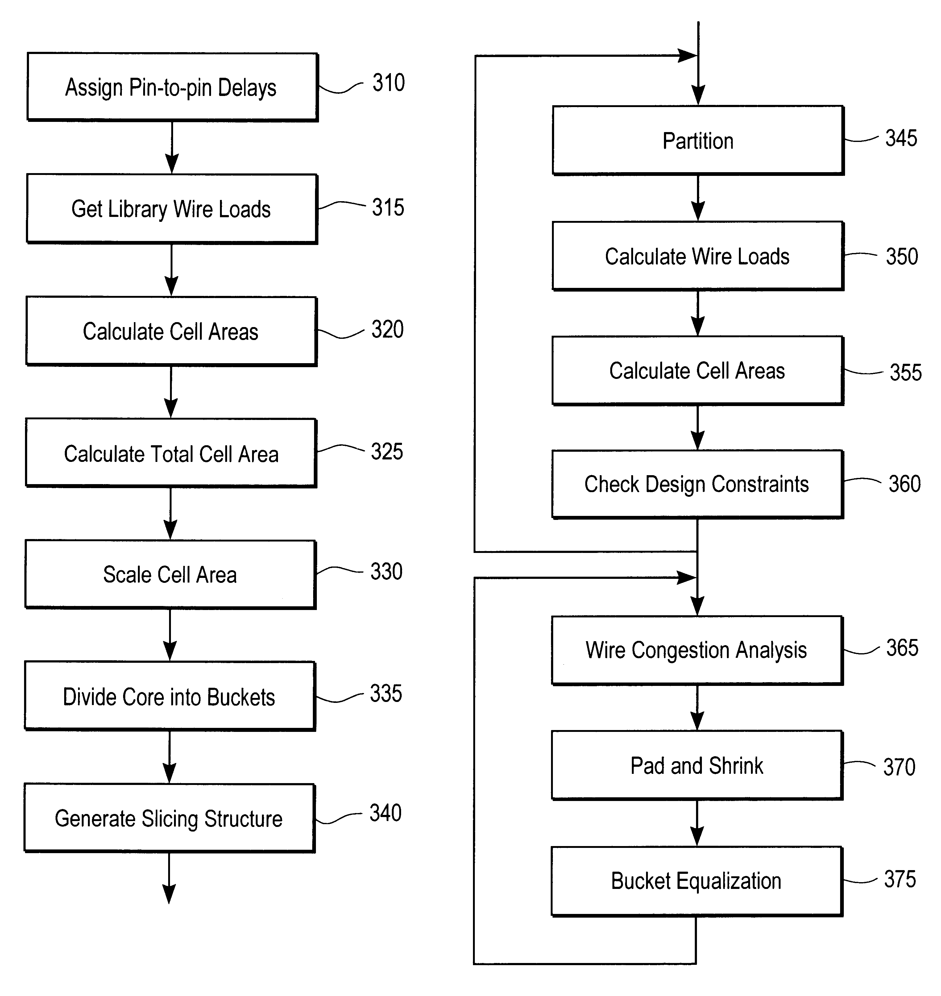
In a constant delay approach to cell placement, the pin-to-pin delay of each cell is fixed early on in the optimization flow. This delay is maintained independently of the load a cell drives. In order to keep delay constant, the size of the cell is adjusted according to the load that it drives. As a result, the area of each cell in the design varies with the load that it drives. The area of each cell is

a=b+s.multidot.c.sub.out (4)

where b and s are constants...


PUM


Abstract

A system for calculating interconnect wire lateral capacitances in an automated integrated circuit design system subdivides the chip area of a circuit design to be placed and routed into a coarse grid of buckets. An estimate of congestion in each bucket is computed from an estimated amount of routing space available in the bucket and estimated consumption of routing resources by a global router. This congestion score is then used to determine the spacing of the wires in the bucket which is in turn used to estimate the capacitance of the wire segment in the bucket.

Description

1. Field of the InventionThe present invention is directed to digital logic design systems. More particularly, the invention is directed to automated digital logic synthesis and placement systems for integrated circuits, and to performance optimization of digital integrated circuits.2. Background of the Related ArtPrior art computer aided design (CAD) systems for the design of integrated circuits (ICs) and the like assist in the design thereof by providing a user with a set of software tools running on a digital computer. In the prior art, the process of designing an integrated circuit on a typical CAD system is done in several discrete steps using different software tools.The design process can be broadly divided into two phases. The initial phase 100 (shown in FIG. 1) of selecting the right components and connecting them so that the desired functionality is achieved is called logical synthesis. The second phase 200, in which the selected components are placed within the confines o...

Claims


Application Information

Patent Timeline
Patent Type & Authority Patents(United States)
IPC IPC(8): G06F17/50
CPCG06F17/5036G06F17/5077G06F17/5072G06F30/392G06F30/394G06F30/367G06F30/3947
Inventor SRINIVAS, PRASANNA VENKATBORAH, MANJITBUCH, PREMAL
Owner MAGMA DESIGN AUTOMATION
Why Eureka
Try Eureka