Composite interposer and method for producing a composite interposer

a composite interposer and interposer technology, applied in the direction of printed circuit manufacturing, cross-talk/noise/interference reduction, printed circuit aspects, etc., can solve the problems of capacitive coupling between the lines and the substrate, noise in the signals, and close proximity of signal lines

Inactive Publication Date: 2003-02-18
FUJITSU LTD
View PDF73 Cites 233 Cited by
  • Summary
  • Abstract
  • Description
  • Claims
  • Application Information

AI Technical Summary

Problems solved by technology

However, problems arise in placing signal lines in close proximity to each other and to power supply lines when fabricating such an interposer.
These problems include interference and cross-talk arising from coupling between the lines on a common layer or between signal lines on different signal layers, and capacitive coupling between the lines and the substrate which produces noise in the signals.
Disadvantages of conventional approaches to packaging IC chips in MCMs arise from the method used to deliver power to the chips.
This problem results because power lines are typically routed through the same substrate which is utilized to carry signals to and from the chip.
This will further increase the problems caused by densely packed signal traces.
Another important disadvantage is that the thinness of the substrates used in traditional multichip modules results in the power feeds to the IC chips having a relatively high impedance.
This results in undesired noise, power loss, and excess thermal energy production.
These problems are relevant to the routing of both power and signal lines though an interposer substrate.

Method used


Image

  • Composite interposer and method for producing a composite interposer
  • Composite interposer and method for producing a composite interposer
  • Composite interposer and method for producing a composite interposer

Examples


Embodiment Construction

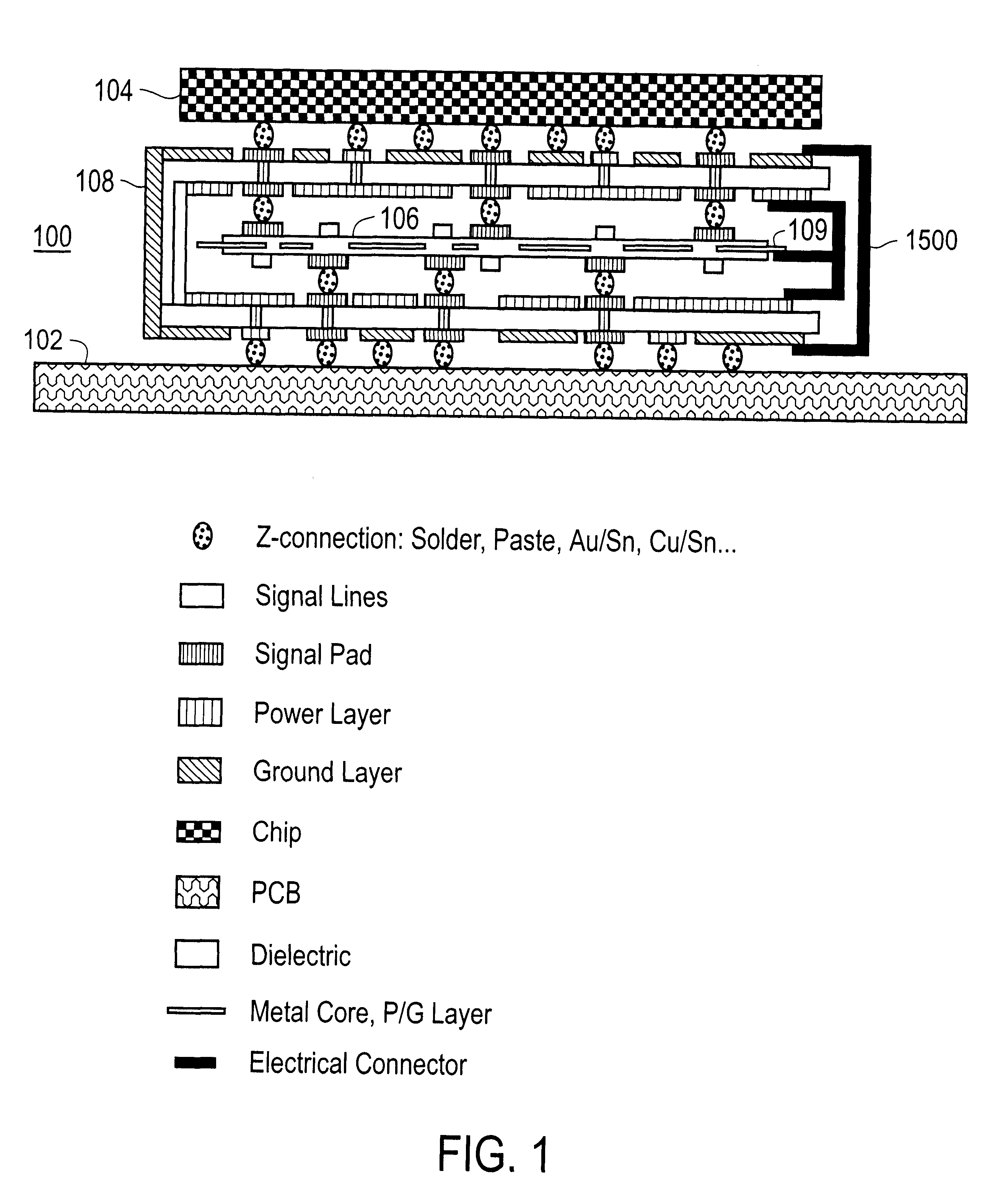
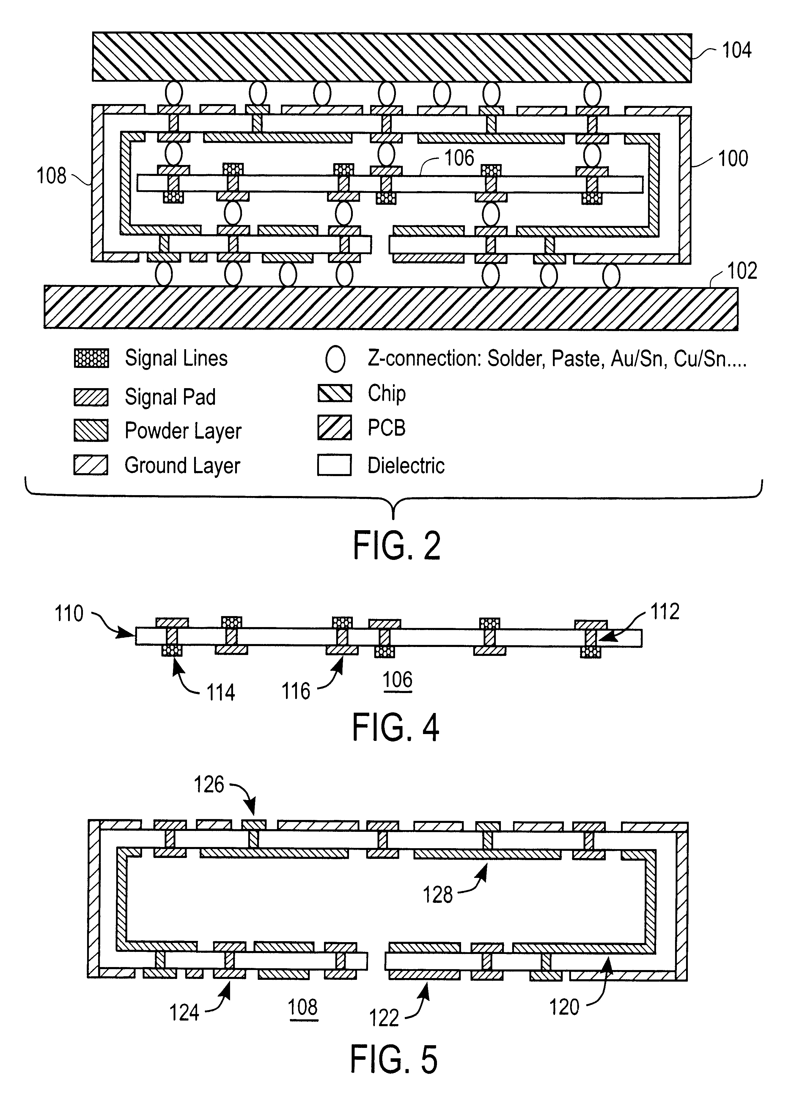
The present invention is directed to an interposer designed to provide signal, power, and ground connections between an integrated circuit chip and an underlying printed circuit board or substrate. The inventive interposer provides the following several advantages over conventional structures:

(1) The density of the interposer signal routing lines can be higher than for conventional interposers because there are no power and ground line connects which pass through the signal core. In this regard, the gap between vias which connect signal lines is increased by approximately a factor of the square root of 2 compared to the line density on a chip. This means that the signal line density on the interposer can be increased relative to that on a chip which includes power and ground lines:

(2) Different technology and processes can be used to fabricate the signal core and the power / ground wrap. Since the pattern size of the power / ground wrap is larger, a lower cost process (e.g., subtractive...


PUM


Abstract

A composite interposer for providing power and signal connections between an integrated circuit chip or chips and a substrate. The interposer includes a signal core formed from a conductive power / ground plane positioned between two dielectric layers. A method for fabricating a composite interposer comprising disposing a silicon layer on a substrate, and selectively etching the silicon layer down to the substrate to develop silicon openings with a silicon profile, and to expose part of the substrate. Vias are formed through the exposed part of the substrate. The method additionally includes filling the vias and the silicon openings with a filler material (e.g., a high-aspect-ratio-capable photodefinable epoxy polymer) to form filled silicon openings and filled vias, forming first openings through the filled silicon openings and through the filled vias, forming second opening through filler material to expose semiconductor devices on the silicon layer, and interconnecting electrically, through the first openings and through the second openings, the exposed semiconductor devices with pads disposed against a bottom of the substrate.

Description

1. Field of the InventionEmbodiments of the present invention relate to integrated circuit device packaging; more specifically, to an interposer substrate capable of reducing cross-talk between signal lines which is suitable for interconnecting integrated circuit chips to a printed circuit board or other substrate. Embodiments of the present inventions also provide a composite interposer and method for producing the composite interposer which may be placed between an integrated circuit and a printed circuit board.2. Description of the Prior ArtAn interposer is a structure used in the manufacture of single and multi-chip modules (SCMs or MCMs) to electrically connect one or more integrated circuit chips (ICs) to a printed circuit board or other substrate. The interposer provides power and ground connections between the board or substrate and the ICs. The interposer also provides signal paths between the IC chips and the board or substrate, and if desired, between different chips moun...

Claims


Application Information

Patent Timeline
Patent Type & Authority Patents(United States)
IPC IPC(8): H01L23/50H01L23/552H01L23/498H01L23/538H01L23/52H01L23/48H05K1/02H05K3/20H05K1/14H01L23/12
CPCH01L23/49822H01L23/49838H01L23/50H01L23/5383H01L23/5385H01L23/5386H01L23/552H05K1/0219H01L23/49833H01L2224/16235H01L2924/01004H01L2924/01046H01L2924/01078H01L2924/01079H01L2924/09701H01L2924/15311H01L2924/3011H01L2924/3025H05K1/141H05K1/144H05K3/20H05K2201/049H05K2201/055H05K2201/10378H01L2924/01019H01L2924/01322H01L2224/16225H01L2924/01327H01L2924/10253H01L2924/00
Inventor PETERS, MICHAEL G.MCCORMACK, MARK THOMASBERNALES, ARIS
Owner FUJITSU LTD
Why Eureka
Try Eureka