Sputtering target for depositing silicon layers in their nitride or oxide form and a process for its preparation

a technology of sputtering target and silicon layer, which is applied in the direction of application, vacuum evaporation coating, coating, etc., can solve the problems of boron or phosphorus doped polycrystalline silicon tiles that are rather brittle and expensive, and the target is in short supply, so as to achieve the effect of high aluminum doping level

Inactive Publication Date: 2003-06-24
HERAEUS MATERIALS TECHNOLOGY GMBH & CO KG
View PDF11 Cites 12 Cited by
  • Summary
  • Abstract
  • Description
  • Claims
  • Application Information

AI Technical Summary

Benefits of technology

Surprisingly, it has been found with sputtering targets comprising these cast silicon-aluminum tiles, which are close to the final size, that silicon oxide or silicon nitride layers can be sputtered with comparable optical parameters despite the casting defects, that are present, such as micro-pores and micro-fissures and despite the high aluminum doping level.

Problems solved by technology

With prior technology, the boron or phosphorus doped polycrystalline silicon tiles have been found to be rather brittle and expensive.
Moreover, such targets are in short supply because they are predominantly produced for photovoltaic wafers, instead of sputtering targets.
U.S. Pat. No. 5,853,816 shows that aluminum can be added to silicon sputter targets but points out that with aluminum insufficient homogeneity cause arcing of the SiAl target.
The tiles produced in this way are more expensive in production, and they are brittle and therefore easily cracked by sputtering or in handling.
A considerable problem occurs because these prior known titles need to be bonded, i.e., soldered, to a metallic backing plate for fixation in the sputter machine.
The reason that such tiles are expensive is because they are produced by a very time consuming melting process and by an expensive cutting and grinding process.

Method used


Image

  • Sputtering target for depositing silicon layers in their nitride or oxide form and a process for its preparation
  • Sputtering target for depositing silicon layers in their nitride or oxide form and a process for its preparation

Examples


example

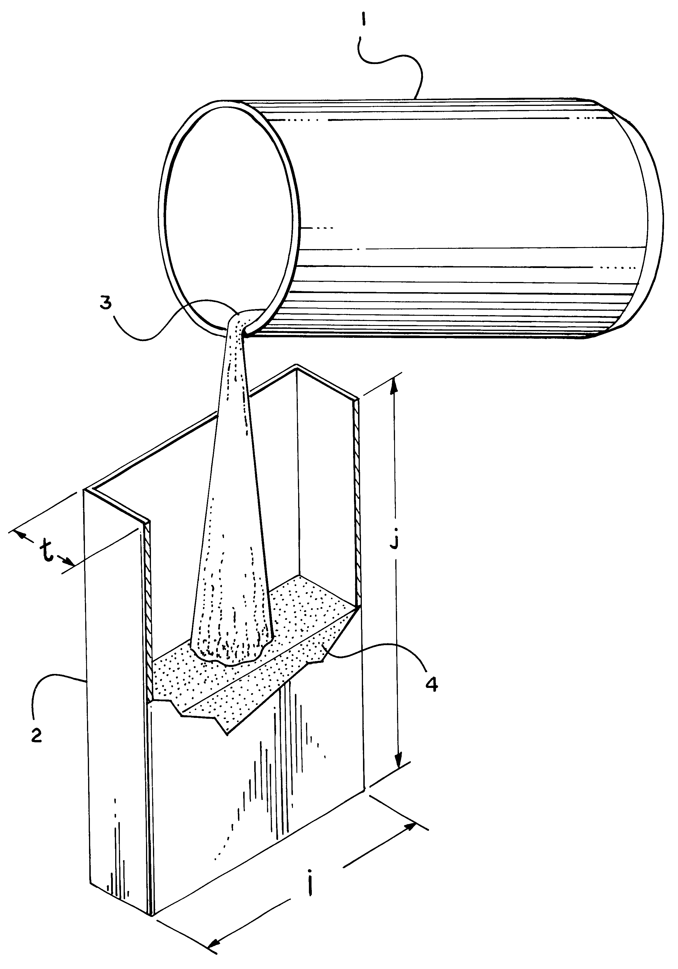
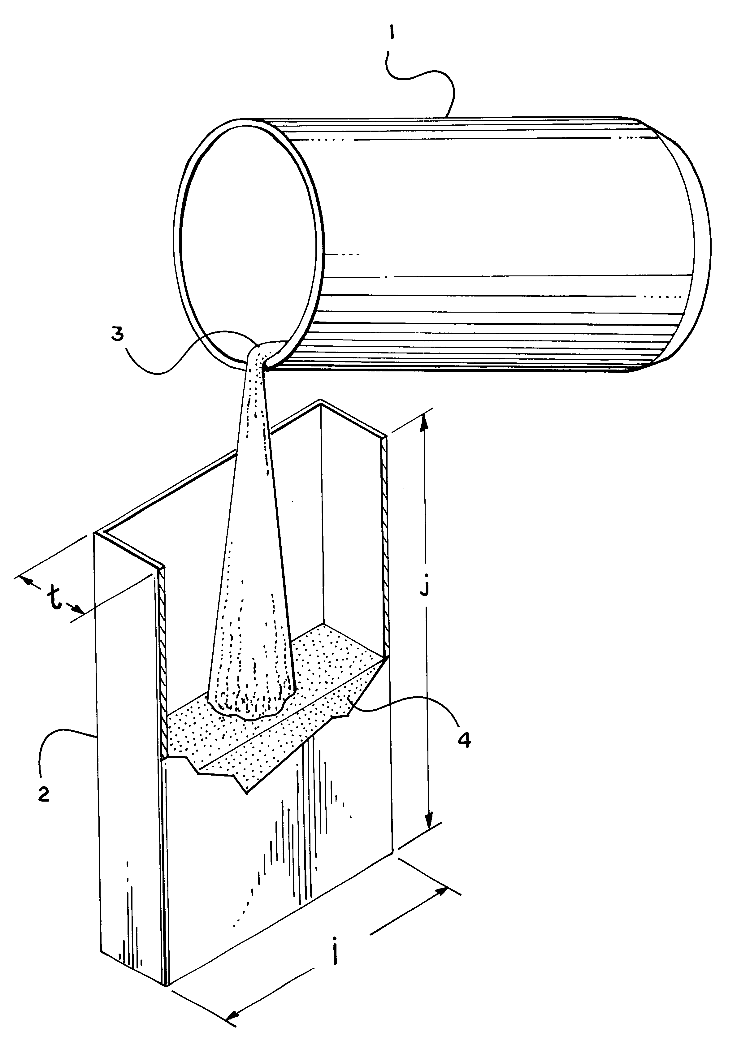
Various alloys, which comprised industrially pure silicon and aluminum, i.e. 99.5% purity with respect to the metal in each case, were melted in a vacuum induction oven. Graphite was used as the crucible material. The receptacle used as the casting mold had the following dimensions: width 110 mm, thickness 16 mm and height 330 mm. The casting mold, of graphite was preheated to approximately 200.degree. C. and was introduced into the vacuum oven through sluices directly before casting.

The following alloys were melted:

a) Si 99.5% purity without Al doping

b) Si 99.5% purity+1 wt % Al

c) Si 99.5% purity+5 wt % Al

d) Si 99.5% purity+10 wt % Al

e) Si 99.5% purity+15 wt % Al

The purity of the aluminum is 2N5 to 5N purity.

Whereas with pure silicon (Example a), only completely broken up cast components were capable of being prepared, even after varying the deposition conditions, it was possible to produce intact plates starting from alloying levels of only 1 wt % Al. However, the cast plates with...


PUM

PropertyMeasurementUnit
temperatureaaaaaaaaaa
poweraaaaaaaaaa

Abstract

The target material for a sputtering target for depositing silicon layers in their nitride or oxide form by means of reactive cathode atomization, such as e.g. Si3N4 or SiO2 in the form of optical functional layers or in the form of thermal protective layers on glass substrates, is a cast silicon element, that has been solidified from the melt condition and which forms a parallelepiped, with a dopant, that has been mixed in with the melt, whereby the dopant is 1 wt % to 15 wt % aluminum, and whereby the casting mold preferably has a cavity which forms a parallelepiped.

Description

INTRODUCTION AND BACKGROUNDThe present invention relates to a sputtering target for depositing silicon layers in their nitride or oxide form by means of reactive cathode atomization, such as e.g. Si.sub.3 N.sub.4 or SiO.sub.2 in the form of optical functional layers on glass substrates. More particularly, according to the present invention, the target material is a cast silicon element, that has been solidified from the melt condition, with an additive mixed in with the melt. In another aspect, the present invention relates to a process for preparation of the aforesaid sputtering target and products obtained therebyThin silicon layers in their nitride and oxide form are becoming increasingly important in modern glass coating processes. In particular, the technology is important in the fields of optical coatings on large glass surfaces, as well as architectural, automotive and anti-reflective glass. These layers are usually applied by means of sputtering technology. A Si.sub.3 N.sub....

Claims


Application Information

Patent Timeline
Patent Type & Authority Patents(United States)
IPC IPC(8): B22D25/00C23C14/34
CPCC23C14/3414B22D25/00
Inventor WEIGERT, MARTINKONIETZKA, UWE
Owner HERAEUS MATERIALS TECHNOLOGY GMBH & CO KG
Why Eureka
Try Eureka