Autocalibration of the A/D converter within the CMOS type image sensor

a technology of a/d converter and image sensor, which is applied in the direction of code conversion, instruments, television systems, etc., can solve the problems of varying degrees of parasitic effects of analog signals generated by each light detecting element, high cost of integrated circuit chips containing a ccd image sensor, etc., and achieve the effect of minimizing parasitic effects and distortion of a/d converters and cds circuits

Inactive Publication Date: 2003-06-24
ALCOR MICRO CORP
View PDF3 Cites 57 Cited by
  • Summary
  • Abstract
  • Description
  • Claims
  • Application Information

AI Technical Summary

Benefits of technology

An active pixel image sensor fabricated by a CMOS process is described herein, which includes a two-dimensional pixel array core of photo sensing diodes whose conductivities are related to the magnitude of light impinging upon the photodiodes. The analog signals generated by the photodiodes are buffered through a source follower amplifier, accessed by row transistors and coupled to respective columns in the array. The analog signals at each column line are converted to digital signals by an A/D converter (ADC) connected to each column line. Among other methods, the A/D converter may be formed by a high-gain comparator, an 8-bit binary counter coordinated with a reference ramp signal synchronized with a specific timing sequence. A specific timing sequence is used to allow the A/D converter circuit to implement the A/D conversion within a time frame, so that all the sensing elements in a row will have their respective light level converted into a digital value during this interval. ...

Problems solved by technology

Integrated circuit chips containing a CCD image sensor are expensive due to the specialized process required.
The CCD also consumes a relatively large power dissipation because of the clock signals that are required and the high voltage that is usually needed.
However, it has been discovered by the inventor that, for large area and high density pixel arrays, the analog signal generated by each light detecting element is subject to varying degrees of parasitic effects such as those caused by parasitic capac...

Method used


Image

  • Autocalibration of the A/D converter within the CMOS type image sensor
  • Autocalibration of the A/D converter within the CMOS type image sensor
  • Autocalibration of the A/D converter within the CMOS type image sensor

Examples


Embodiment Construction

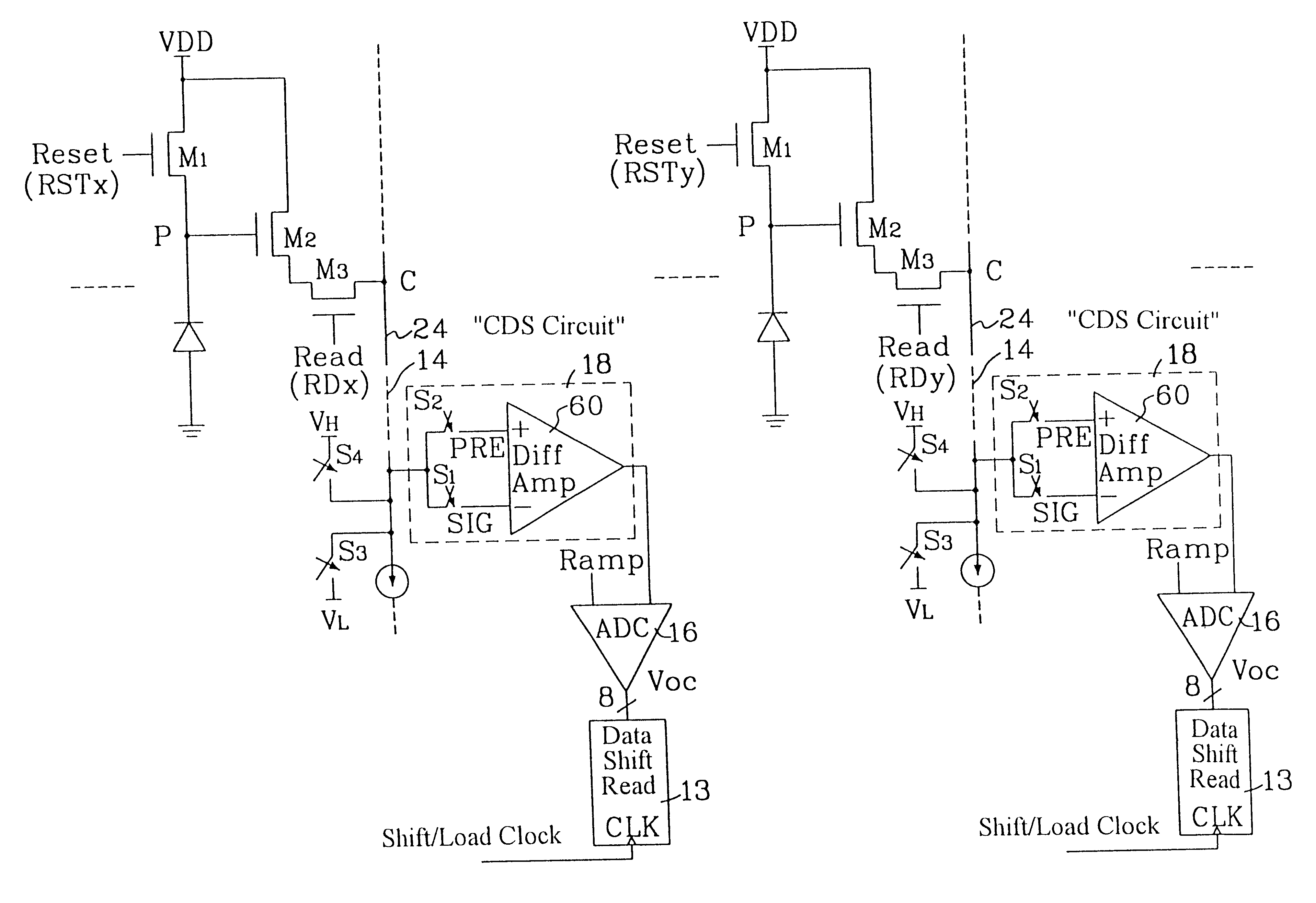
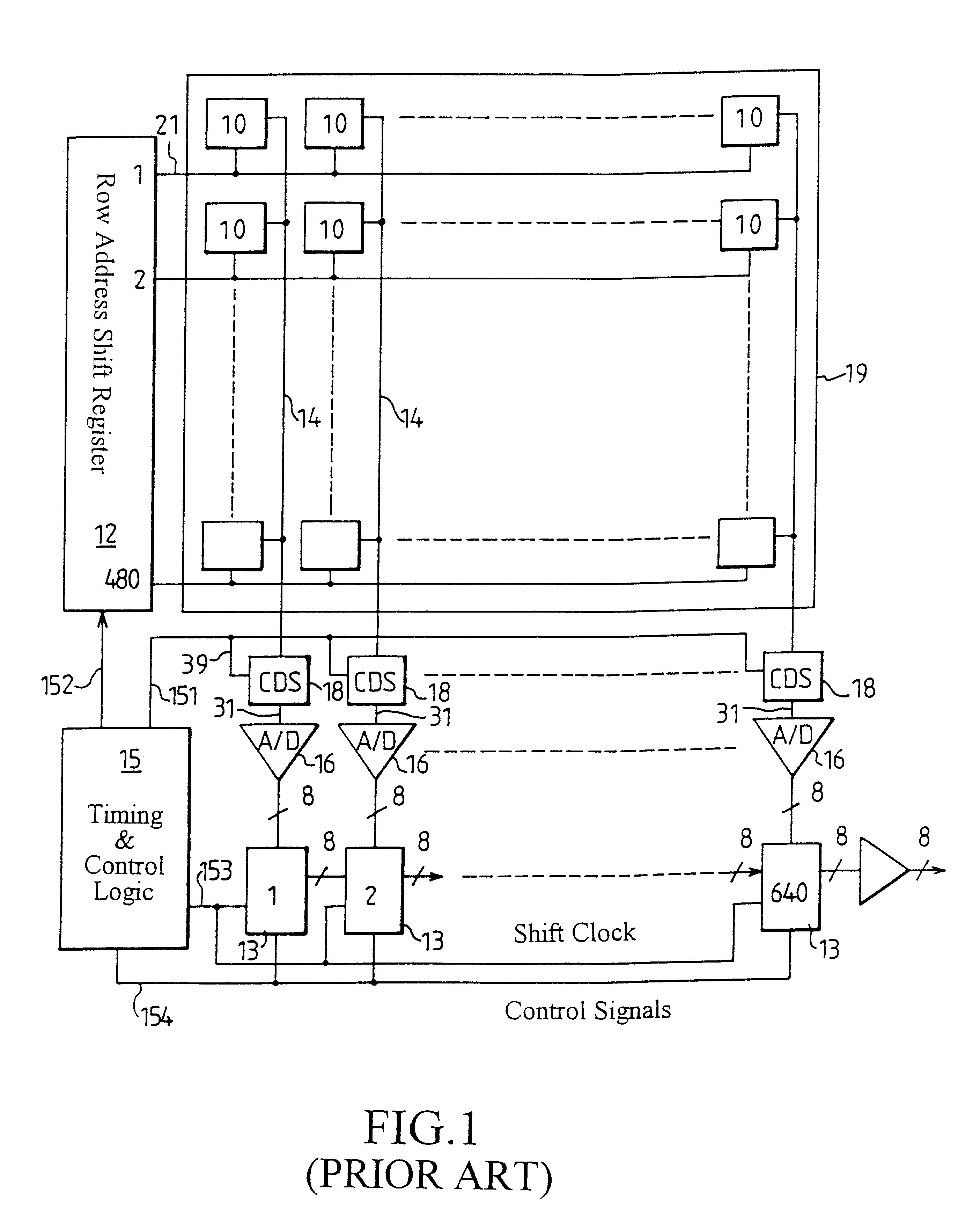
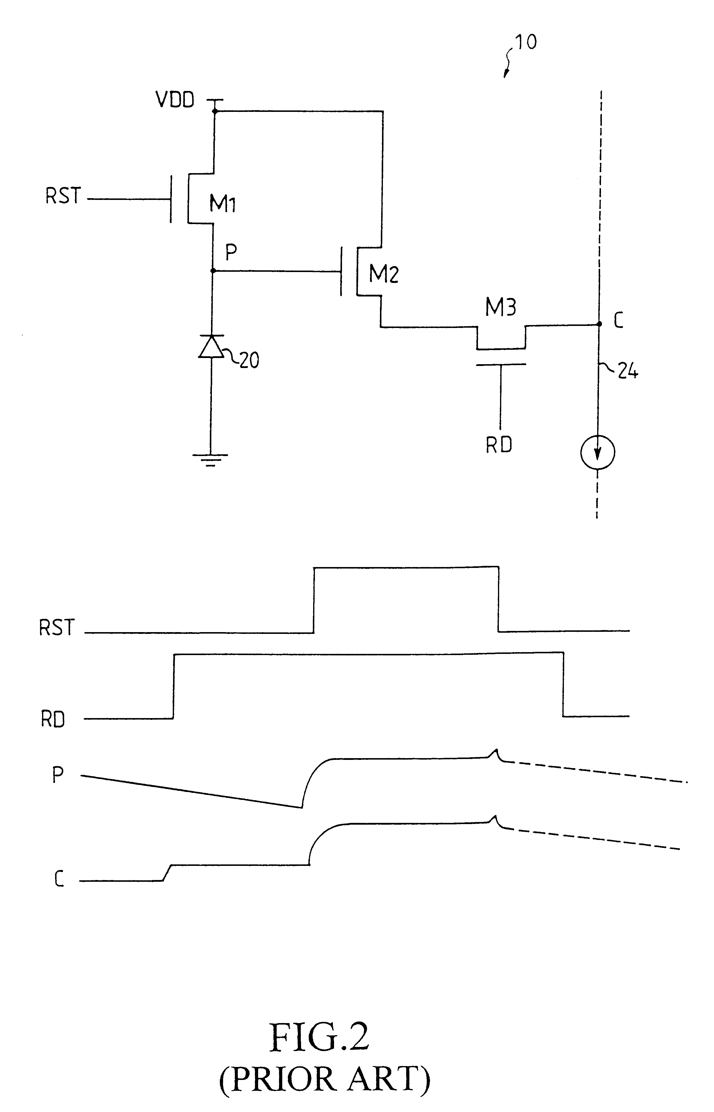
FIG. 1 illustrates the architecture of a 640.times.480 CMOS active pixels image sensor formed on a single integrated circuit chip. The image sensor core 19 comprises a two-dimensional pixel array of light detecting elements 10 which include identical circuitry shown in FIG. 2. A row address shift register 12, with its control signals coming from the timing / control logic 15, is connected to the core array 19 to address one row at a time. The output of shift register 12 addresses the core array 19 row-by-row to read the analog signal into the column lines 14 according to a predetermined frame rate timing requirement.

In one embodiment, each A / D converter 16 is connected to receive an analog signal, via a well-known correlated-double sampling (CDS) circuit 18, from corresponding column line 14 and convert each analog signal to a digital signal representative of gray level of light intensity detected by the respective pixel element 10. For example, if an eight-bit A / D conversion is imple...


PUM


Abstract

A method for initializing a counter within a corresponding set of A/D converters of N sets of A/D converters of a single-chip CMOS-type image sensor in order to minimize none uniformity across the N sets of A/D converters is provided. The single chip CMOS type image sensor includes an image sense array having N columns of output lines for outputting N analog signals respectively; and a signal process device for generating N sets of digital signal each of which corresponds to one of N analog signals respectively. The signal process device has N input lines and N sets of A/D converter each of which including a counter for generating one of the N sets of digital signal respectively. The method comprises the steps of applying a predetermined reference voltage at each of N input lines of the signal process device such that a compensation value corresponding to each set of A/D converter is obtained. The method further preloads the counter of each corresponding set of A/D converter with the compensation value corresponding to each set of A/D converter.

Description

The present invention relates to a CMOS type image sensor and, in particular, to an initialization procedure of the A / D within the CMOS type image sensor.BACKGROUND OF INVENTIONAn image sensor is used to transform an optical image focused on the sensor into an electrical signal. The image sensor typically contains an array of light-detecting elements, where each element produces a signal in response to the light intensity impinging on that element when an image is focused on the array. These signals may then be used to display a corresponding image on a monitor.One very well-known type of image sensor is a charge coupled device (CCD). Integrated circuit chips containing a CCD image sensor are expensive due to the specialized process required. The CCD also consumes a relatively large power dissipation because of the clock signals that are required and the high voltage that is usually needed. In contrast to the CCD image sensor, CMOS active pixel sensors (APS) have attracted much atte...

Claims


Application Information

Patent Timeline
IPC IPC(8): H03M1/10H03M1/56H03M1/12H03M1/50H04N5/30
CPCH03M1/1023H03M1/123H04N5/378H04N5/3742H03M1/56H04N25/767H04N25/75H04N5/30
Inventor LEE, SYWE N.
Owner ALCOR MICRO CORP
Why Eureka
Try Eureka