Magnetic sensor, magnetic sensor apparatus, semiconductor magnetic resistance apparatus, and production method thereof

a magnetic sensor and semiconductor technology, applied in the field of magnetic sensor, magnetic sensor apparatus, semiconductor magnetic resistance apparatus, and production method thereof, can solve the problems of difficult to meet strict requirements, difficult to drive, and inability to pick up electrical noise from magnetic sensors using insb

Inactive Publication Date: 2003-07-08
ASAHI KASEI KK +1
View PDF9 Cites 37 Cited by
  • Summary
  • Abstract
  • Description
  • Claims
  • Application Information

AI Technical Summary

Problems solved by technology

However, InSb has a problem that it is difficult to meet the strict requirements of the recently expanding applications of magnetic sensors.
However, since resistance of a magnetic sensing part greatly depends on temperature, at low temperatures of, below -40.degree. C., a magnetic sensor using InSb becomes liable to pick up electrical noises due to considerable increase in resistance of the device.
Further, at high temperatures exceeding 120.degree. C. increases in drive current because of a large decrease in device resistance results in driving difficulty.
C. As a result, variation of self resistance in effect becomes a variation of input resistance of the magnetic sensor, and as a result, at high temperatures, a breakdown or the like due to eddy current is generated, a higher drive input current becomes required, and in a small-sized integrated drive circuit, stable drive of the device becomes difficu
lt. That is, a complex, expensive drive circuit is requi
Further, at low temperatures, device resistance becomes very high, which results in a strong influence of stray magnetic noise or causes misoperation due to noise As a result, the magnetic sensor is usable only in very limited cases, and its merit as a non-contact sensor, hasp not been sufficiently utilized.
When such a magnetic sensor, a power supply for driving the magnetic sensor, and a control circuit of the magnetic sensor for amplifying the magnetic field detection output are attempted to be realized in a small size, at a low cost, and with high performance, such a temperature dependence of resistance due to the material is a great problem.
Further, in driving the magnetic sensor in a wide temperature range from low to high temperatures, a large thermal stress is exerted through a package of the magnetic sensor.

Method used


Image

  • Magnetic sensor, magnetic sensor apparatus, semiconductor magnetic resistance apparatus, and production method thereof
  • Magnetic sensor, magnetic sensor apparatus, semiconductor magnetic resistance apparatus, and production method thereof
  • Magnetic sensor, magnetic sensor apparatus, semiconductor magnetic resistance apparatus, and production method thereof

Examples


embodiment 1

(Embodiment 1)

A Hall device was produced using the following procedures.

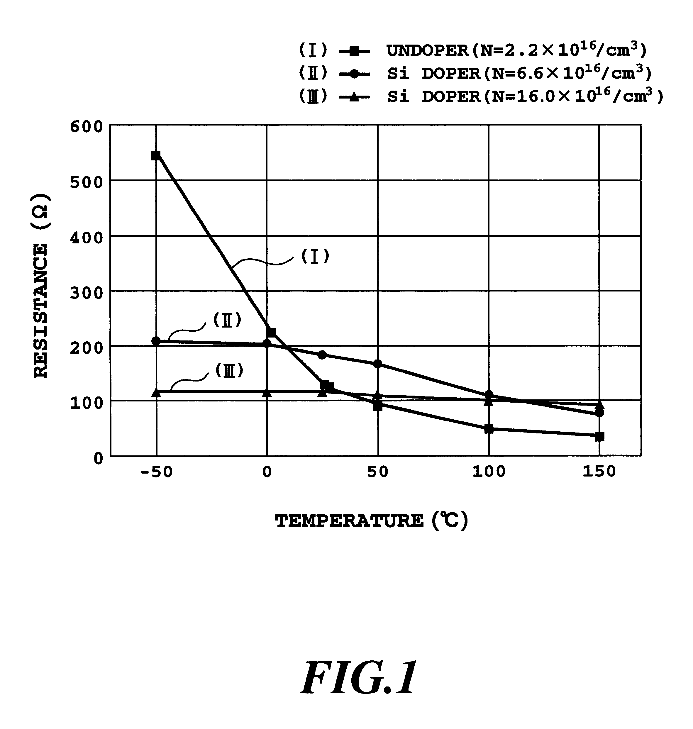
In the present embodiment, a thin film production apparatus specially fabricated for compound semiconductor thin film production was used. The basic construction of the apparatus involves use of a super-high-vacuum chamber, a holder for setting a substrate and a heating control apparatus capable of heating the substrate at a constant temperature. Further a plurality of evaporation sources (Knudsen cells) capable of separately controlling the vapor pressures of materials such as In, Sb, As and the like are provided. In this apparatus, time-series evaporation control of the vapor pressures of the respective materials, and according to a heating program of the substrate by the substrate heating apparatus, single crystal growth of a desired material uniformly on the substrate can be carried out. In addition to the above functions, as necessary, a thin film production apparatus provided with doping means capable of v...

embodiment 2

(Embodiment 2)

A Hall device in which the semiconductor thin film layer is doped with Si was produced using the following procedures.

Specifically, in the present embodiment, a thin film production apparatus specially fabricated for compound semiconductor thin film production was used. The basic construction of the fabrication apparatus includes a super-high-vacuum chamber, a holder for setting a substrate and a heating control apparatus capable of heating the substrate at a constant temperature, and a plurality of evaporation sources (Knudsen cells) capable of separately controlling the vapor pressures of materials such as In, Sb, As and the like. In this apparatus, time-series evaporation control of the vapor pressures of the respective materials, and according to a heating program of the substrate by the substrate heating apparatus, single crystal growth of a desired material uniformly on the substrate can be carried out. In addition to the above functions, as necessary, a thin fil...

embodiment 3

(Embodiment 3)

A bridge-formed magnetic resistance device was produced as follows.

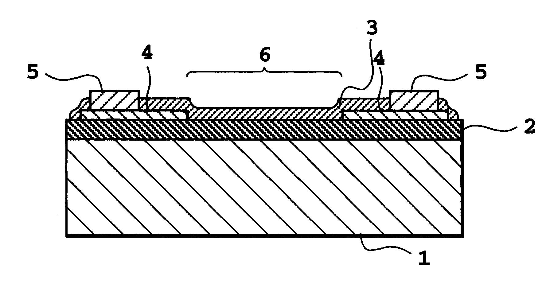
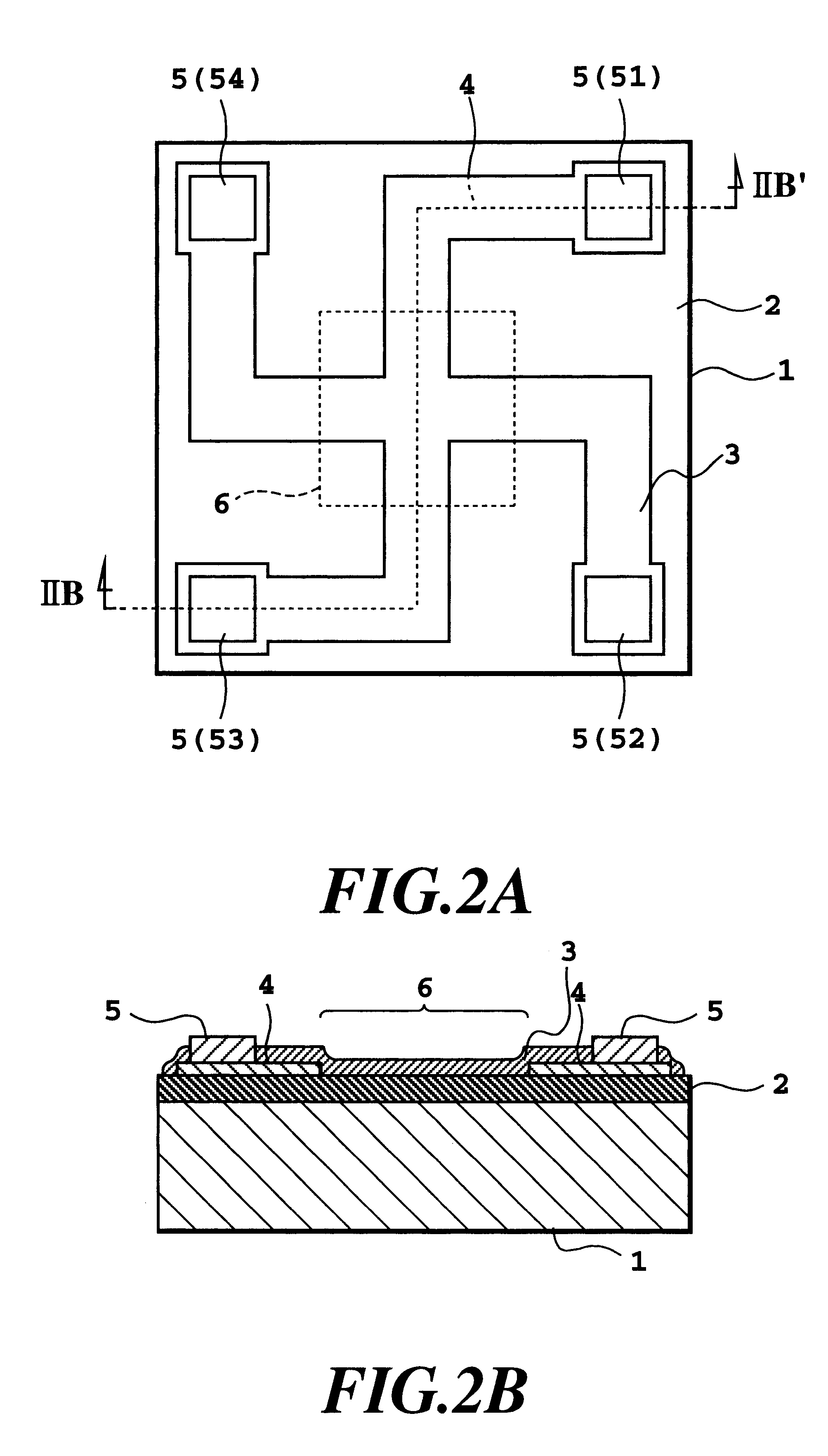
As in Embodiment 2, a Si-doped InSb thin film and an intermediate layer the same as in Embodiment 2 were formed on a flat surface, semi-insulating GaAs substrate. The thus formed 1.0 micron thick InSb thin film had an electron mobility of 35,000 cm / Vsec, and an electron concentration of 7.times.10.sup.16 / cm.sup.3. Next, to form an intermediate layer and an InSb thin film into the desired patter as shown in FIG. 5, a resist film was formed and etched as in Embodiment 2. Part of the intermediate layer was removed by photoetching to form short bar electrodes comprising a plurality of thin metal thin films, a wiring part, and bonding electrodes on the InSb thin film.

Next, as in Embodiment 2, a gold layer was formed only on the surface of the bonding electrodes. Thus, a plurality of bridge-formed magnetic resistance devices of the present invention were simultaneously produced on a single substrate, having ...


PUM

PropertyMeasurementUnit
electron mobilityaaaaaaaaaa
thicknessaaaaaaaaaa
thicknessaaaaaaaaaa

Abstract

An InxGa1-xAsySb1-y (0<x<=1, 0<=y<=1) thin film of an electron concentration of 2x10¹⁶/cm3 or more is formed on a dielectric substrate. Temperature dependence of resistance is controlled by composition setting or donor atom doping of the thin film to reduce the temperature dependence. As a result, a magnetic sensor of small temperature dependence of device resistance and high sensitivity can be provided.

Description

The present invention relates to a semiconductor thin film magnetic sensor and production method thereof.DESCRIPTION OF BACKGROUND ARTMagnetic sensors, such as a magnetic resistance device or a Hall device, using a compound semiconductor thin film with a high electron mobility, such as InSb, are capable of detecting a static magnetic field, and are capable of detecting a rotational angle or speed even at a high or low rotational speed. Therefore, such sensors are widely used as magnetic sensors for small-sized DC motors.However, InSb has a problem that it is difficult to meet the strict requirements of the recently expanding applications of magnetic sensors. For example, a magnetic sensor using InSb has a high sensitivity and exhibits very good characteristics in the vicinity of room temperature. However, since resistance of a magnetic sensing part greatly depends on temperature, at low temperatures of, below -40.degree. C., a magnetic sensor using InSb becomes liable to pick up ele...

Claims


Application Information

Patent Timeline
Patent Type & Authority Patents(United States)
IPC IPC(8): G01R33/06G01R33/09H01L43/00H01L43/10
CPCG01R33/06H01L43/10G01R33/09Y10T428/11H10N50/85H10N52/00
Inventor SHIBASAKI, ICHIROOKAMOTO, ATSUSHIYOSHIDA, TAKASHIOKADA, ICHIRO
Owner ASAHI KASEI KK
Why Eureka
Try Eureka