Semiconductor integrated circuit

a technology of integrated circuits and semiconductors, applied in the direction of individual semiconductor device testing, pulse techniques, instruments, etc., can solve the problems of power consumption in standby mode, inability to establish i.sub.ddq test methods, and difficulty in mass production of these systems

Inactive Publication Date: 2003-08-05
TEXAS INSTR INC
View PDF4 Cites 30 Cited by
  • Summary
  • Abstract
  • Description
  • Claims
  • Application Information

AI Technical Summary

Problems solved by technology

Consequently, power consumption in the standby mode is a problem.
However, for the aforementioned conventional multi-threshold voltage system, the I.sub.ddq test method has not been established.
Consequently, it is hard to use this system for mass production.
As a result, not only the layout area of the semiconductor integrated circuit is increased, but also the power consumption due to the booster circuit in the standby mode becomes a problem.

Method used


Image

  • Semiconductor integrated circuit
  • Semiconductor integrated circuit
  • Semiconductor integrated circuit

Examples


first embodiment

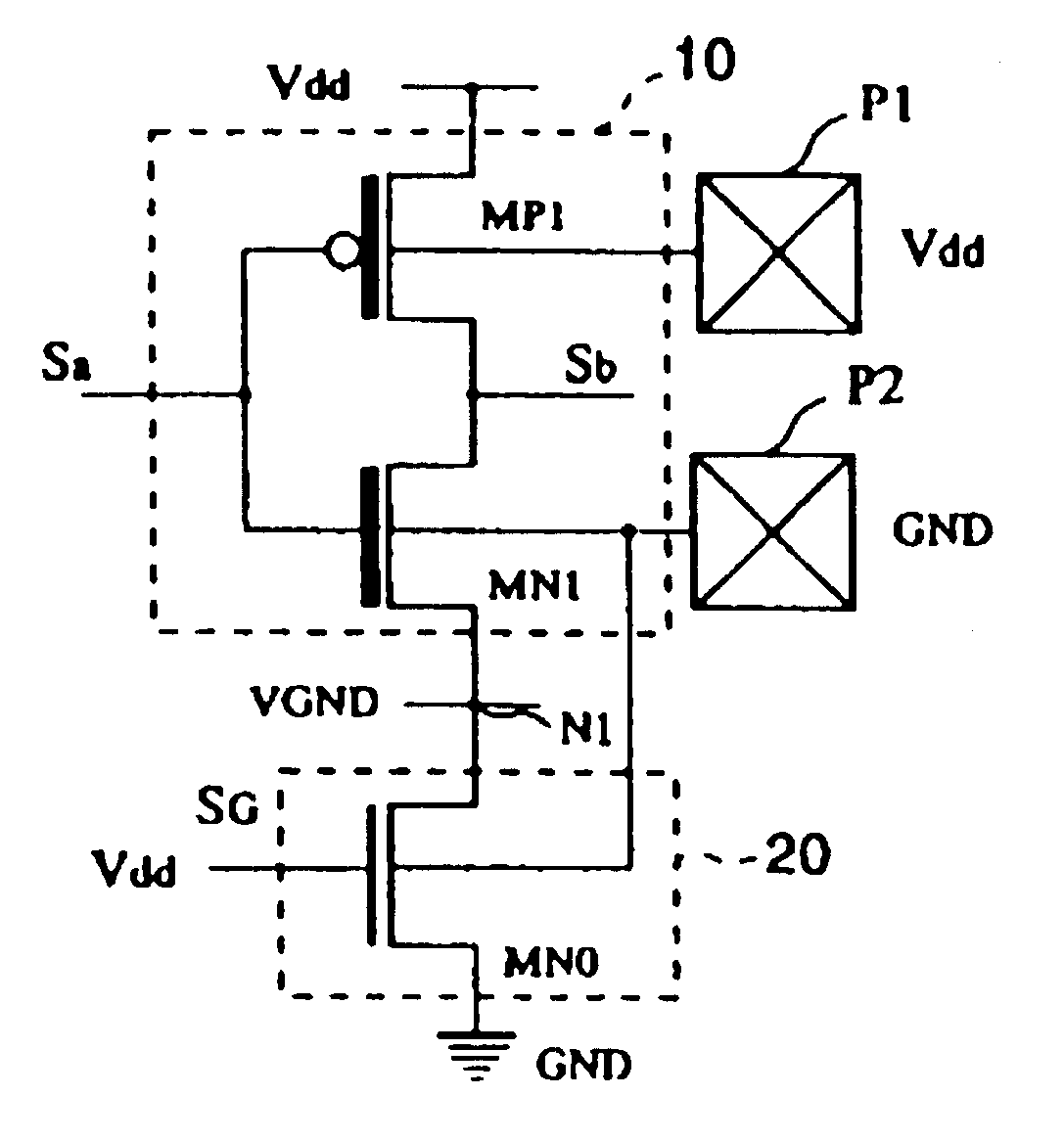
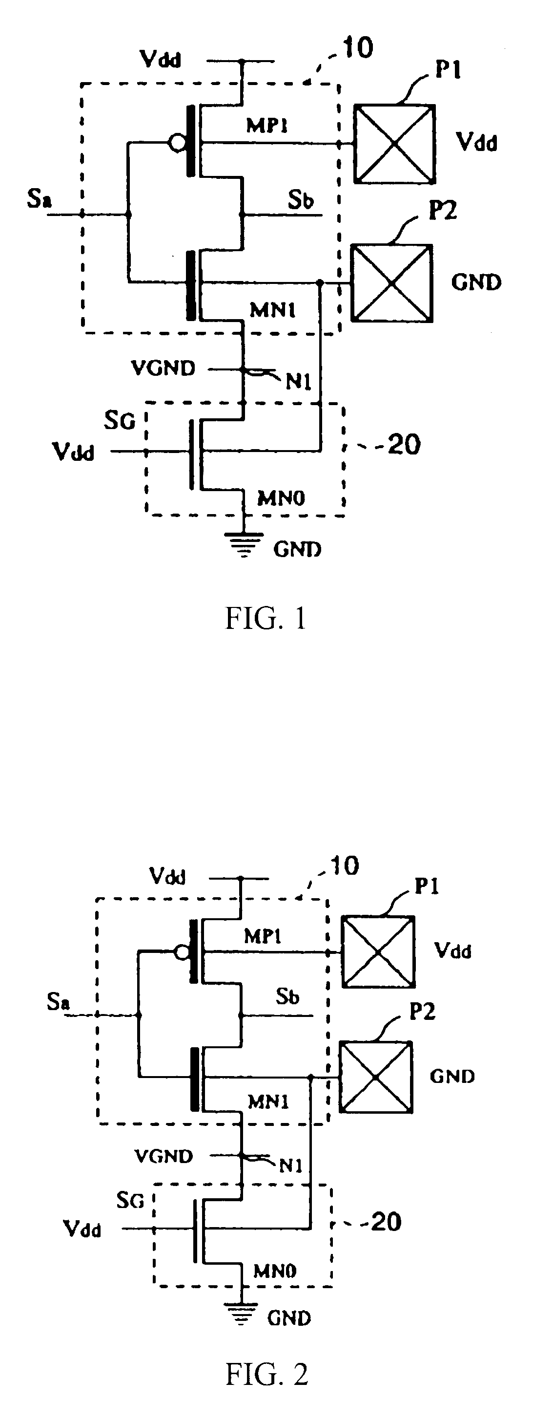
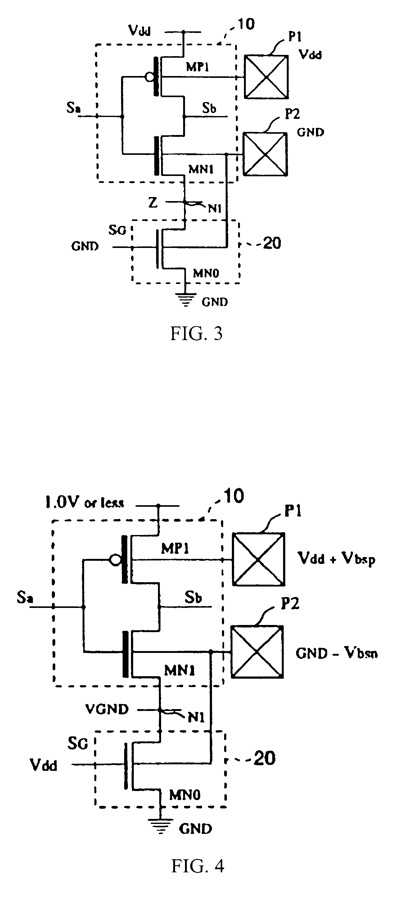
FIG. 1 is a circuit diagram illustrating the semiconductor integrated circuit pertaining to this invention.

As shown in this figure, the semiconductor integrated circuit in this embodiment is composed of logic circuit 10 and switching circuit 20.

Logic circuit 10 is a functional circuit having the prescribed processing function. Logic circuit 10 shown in FIG. 1 is composed of a CMOS inverter which outputs signal Sb that represents the logic inversion value with respect to input signal Sa. However, this invention is not limited to this scheme. It is also possible to be other logic circuits, such as the AND circuit, OR circuit, exclusive-OR (EXOR) circuit, or functional circuits having processing functions other than the logic circuits.

As shown in the figure, logic circuit 10 is composed of PMOS transistor MP1 and NMOS transistor MN1 that are connected in series between the feeding terminal of power source voltage V.sub.dd and node N1 as the feeding terminal of the virtual ground potent...

second embodiment

FIG. 11 is a circuit diagram illustrating the second embodiment of the semiconductor integrated circuit of this invention. The semiconductor integrated circuit in this embodiment is a latch circuit composed of low threshold voltage transistors.

As shown in the figure, this latch circuit is composed of PMOS transistors PT1, PT2, PT3, PT4, NMOS transistors NT1, NT2, NT3, NT4, low threshold voltage PMOS transistor MP1, low threshold voltage NMOS transistor MN1, inverters INV1, INV2, and transfer gate TG1.

The input terminal of inverter INV1 is connected to data input terminal T.sub.in, and its output terminal is connected to node ND1. Also, inverter INV1 (not shown in the figure) is composed of, a low threshold voltage PMOS transistor and a low threshold voltage NMOS transistor. The source of the PMOS transistor is connected to the drain of transistor PT1, and the source of said NMOS transistor is connected to the drain of transistor NT1.

Control signal SLP is applied to the gate of trans...

third embodiment

FIG. 12 is a circuit diagram illustrating the third embodiment of the semiconductor integrated circuit of this invention. The semiconductor integrated circuit in this embodiment is an SRAM composed of low threshold voltage MOS transistors.

As shown in the figure, SRAM is composed of write circuit WR, precharge circuit PRC, memory cell MC, and sense amplifier SA.

Write circuit WR is composed of NOR gates NR1, NR2 made of NMOS transistors NT1, NT2 and transistors having standard threshold voltage.

Inverted signal xWE of write enable signal WE is input to one input terminal of NOR gate NR1, while write data Data is input to the other input terminal. Inverted signal xWE of write enable signal WE is applied to one input terminal of NOR gate NR2, while the logic inverted value xData of write data Data is input to the other input terminal.

The source of transistor NT1 is connected to ground potential GND, its drain is connected to bit line BL, and its gate is connected to the output terminal o...


PUM


Abstract

The objective of this invention is to provide a type of semiconductor integrated circuit which can lessen solution in the circuit area to the minimum necessary level, and can lessen the leakage current in the standby state so as to cut the power consumption, and which allows Iddq test to determine whether it is passed or defective. Logic circuit 10 composed of low threshold voltage transistors and switching circuit 20 composed of transistors having the standard threshold voltage are set. In the operation, the switching circuit is turned ON, and a driving current is fed to logic circuit 10. On the other hand, in the standby mode, the switching circuit is turned OFF, and the path of the leakage current is cut off to lessen generation of the leakage current. In the case of Iddq test, different bulk bias voltages are applied to the channel regions of PMOS transistors and NMOS transistors from an IC tester through pads P1 and P2. In this way, the leakage current can be lessened on a low level, and whether the semiconductor integrated circuit is passed or defective can be judged from the results of the current measurement.

Description

This invention pertains to a type of semiconductor integrated circuit that contains a functional circuit made of CMOS transistors, such as a logic circuit for performing the prescribed logic operation. In particular, this invention pertains to a type of semiconductor integrated circuit that can be determined to be defective or not by means of the I.sub.ddq test.For a low threshold voltage transistor that is formed with a threshold voltage lower than the conventional voltage node, its leakage current is nevertheless larger than that of the conventional transistor although it is appropriate for performing the low voltage operation. Consequently, power consumption in the standby mode is a problem. In the prior art, various systems have been proposed in order to solve this problem. Among them, there is the system that makes use of the multi-threshold voltage CMOS (MT-CMOS) transistor which has two or more types of transistors having different threshold voltages corresponding to the oper...

Claims


Application Information

Patent Timeline
Patent Type & Authority Patents(United States)
IPC IPC(8): G01R31/28G01R31/30G01R31/317H03K19/003G01R31/26G11C11/413G11C29/12H03K19/00
CPCG01R31/3008G01R31/31721H03K19/00361
Inventor TAKAHASHI, HIROSHIHANDA, OSAMUTAKEGAMA, AKIHIROTOYONOH, YUTAKAAWAKA, KAORUIKENO, RIMONTANAKA, TSUYOSHI
Owner TEXAS INSTR INC
Why Eureka
Try Eureka