Method for providing a fill pattern for an integrated circuit design

a fill pattern and integrated circuit technology, applied in pulse technique, instruments, therapy, etc., can solve the problems of metal below the surface, non-planar surface, and particularly serious dishing effect,

Inactive Publication Date: 2003-08-19
MIND FUSION LLC
View PDF6 Cites 225 Cited by
  • Summary
  • Abstract
  • Description
  • Claims
  • Application Information

AI Technical Summary

Problems solved by technology

When using the CMP procedure to remove unwanted portions of metal layer to leave thin lines of metals as interconnects, problems such as dishing may occur, which leads to a non-planar surface.
The dishing effect is particularly serious when the polishing needs to be carried out until metal is left exclusively in previously etched lines without any metal on the surface of a dielectric layer.
It has been found that a significant overpolish is typically needed, which results in erosion of the dielectric layer and dishing of metal below the surface of the dielectric layer.
Additionally, an uneven topography is introduced on the surface of the semiconductor wafer after the CMP procedure, which will be repeated with slight attenuation after subsequent deposition of dielectric layers problems during subsequent steps of the fabrication process.
The problem with the first method is that it is limited to ASIC designs.
Full custom chip designs cannot use this methodology, as the design tools that implement such method must have "a priori" knowledge of the floor plan and power / ground bus structure.
Unless the full custom design is placed and routed in the same manner as an ASIC, the first method will not work.
However, such tools are limited to generating the "checkerboard" pattern and removing portions of that pattern from areas of the chip with active circuitry and wiring.

Method used


Image

  • Method for providing a fill pattern for an integrated circuit design
  • Method for providing a fill pattern for an integrated circuit design
  • Method for providing a fill pattern for an integrated circuit design

Examples


Embodiment Construction

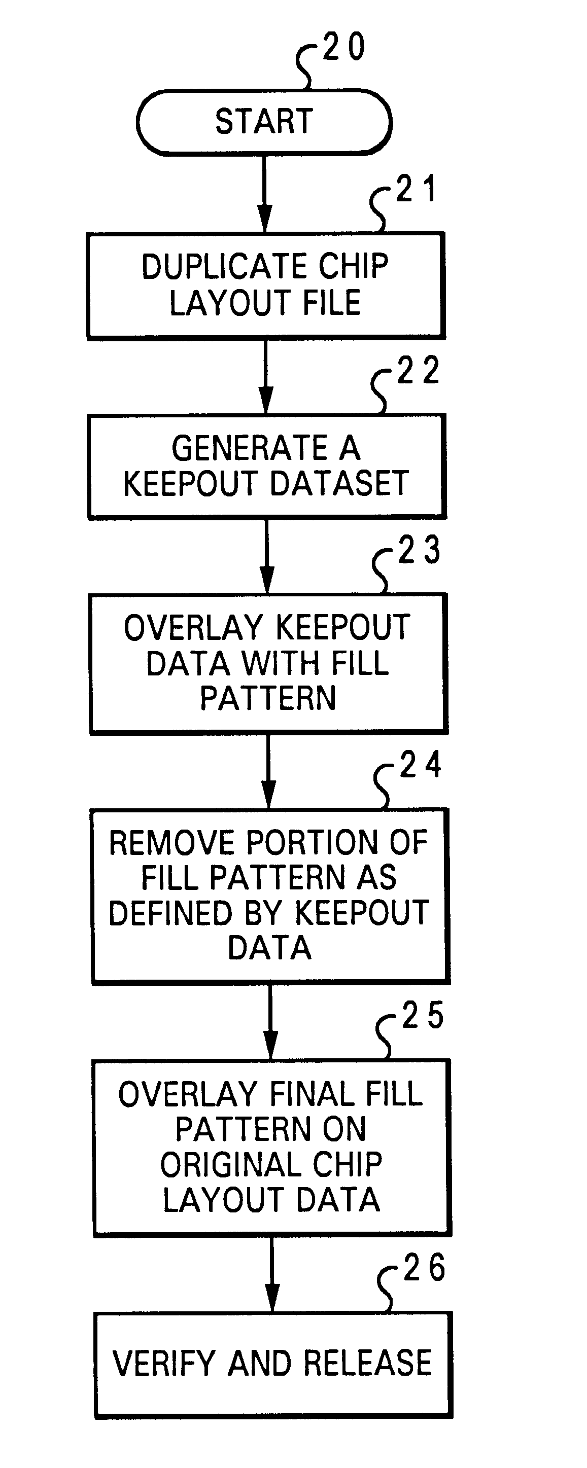
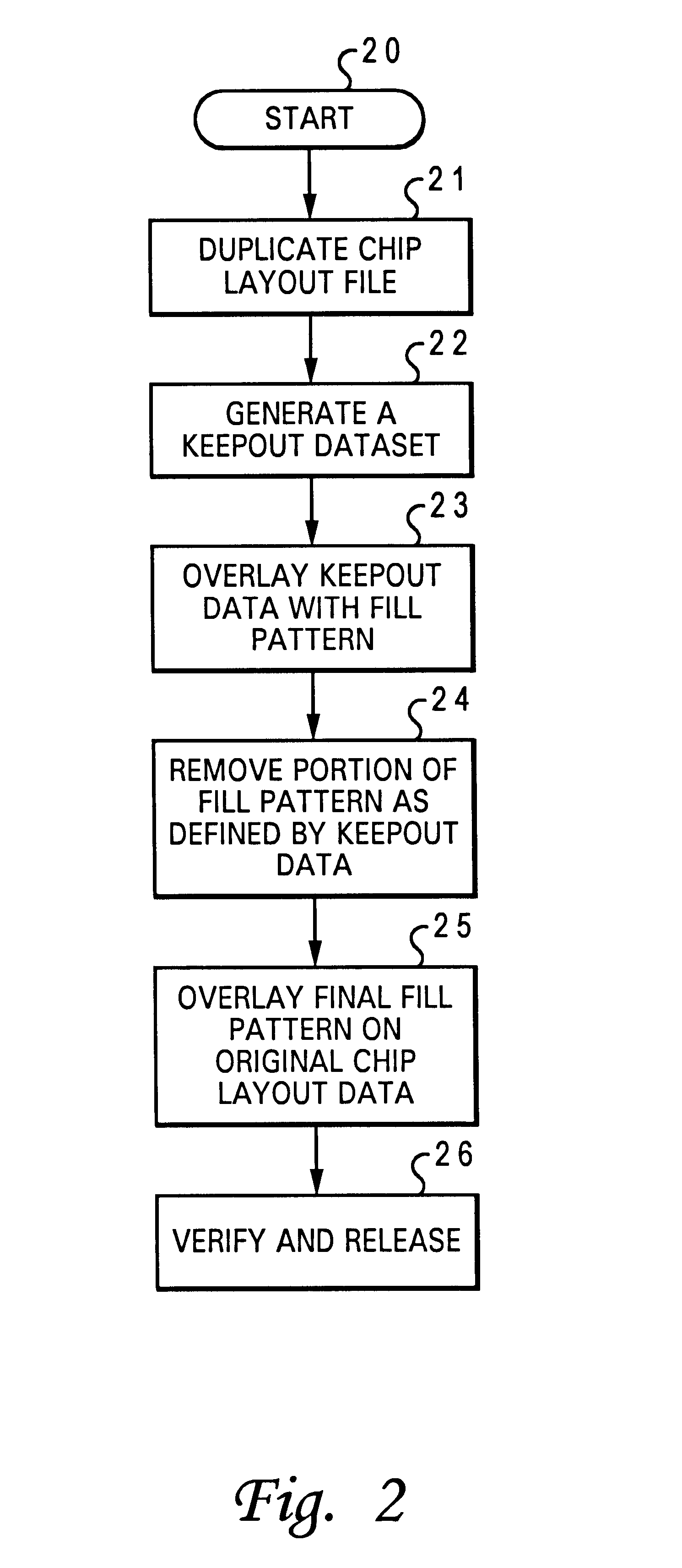
The present invention may be executed in a variety of computers under a number of different operating systems. The computer may be, for example, a workstation, a midrange computer or a mainframe computer. In addition, the computer may be a stand-alone system or part of a network such as a local-area network (LAN) or a wide-area network (WAN). For the purpose of illustration, a preferred embodiment of the present invention, as described below, is implemented on a Unix workstation such as a Sun Ultrasparc Workstation.

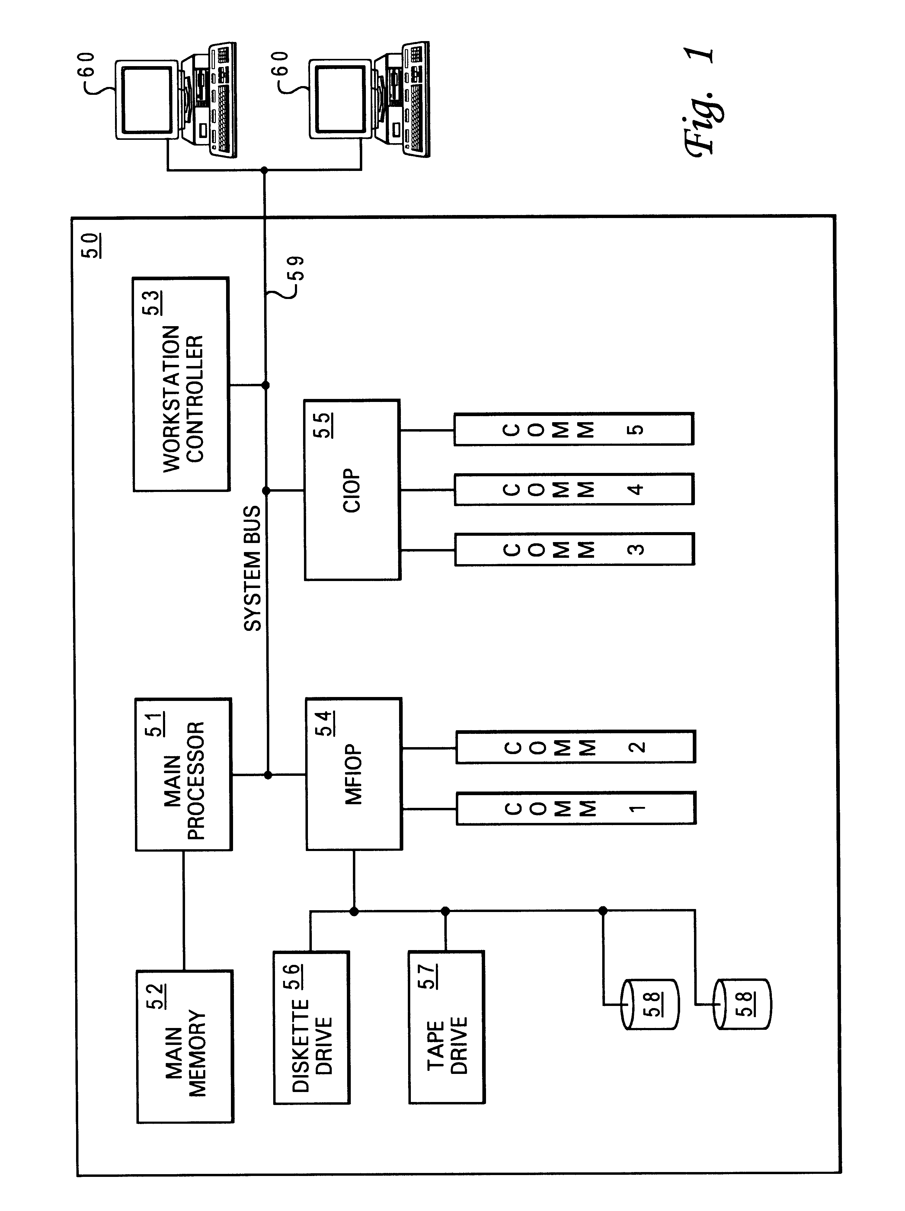
Referring now to the drawings and in particular to FIG. 1, there is illustrated a block diagram of a computer system in which a preferred embodiment of the invention can be executed. Within a computer system 50, a main processor 51 is coupled to a main memory 52 and to a multiple-function I / O processor (MFIOP) 54. Main processor 51 may include a single processor or multiple processors. Several peripheral storage devices such as a diskette drive 56, a tape drive 57, and di...


PUM


Abstract

A method for providing a fill pattern for integrated circuit designs is disclosed. A keepout file having keepout data is generated from a chip design layout file having chip design layout data. The keepout file includes a map of areas of an integrated circuit design where fill patterns cannot be placed. The map of areas from the keepout file is then overlaid with a fill pattern to yield a fill-pattern file. Fill patterns from the fill-pattern file is removed from locations that coincide with locations as defined by the keepout data to yield a final-fill file with crucial fill pattern data. The crucial fill pattern data from the final-fill file is overlaid on the design layout data in the chip design layout file to yield a complete design layout file. Finally, the design rule integrity and logical to physical correspondence of the complete design layout file is verified.

Description

1. Technical FieldThe present invention relates to integrated circuits in general, and in particular to a method for manufacturing integrated circuit devices. Still more particularly, the present invention relates to a method for providing a fill pattern for an integrated circuit design.2. Description of the Prior ArtGenerally speaking, an integrated circuit device is a layered interconnected structure formed by a series of processing steps during which metallization, dielectrics, and other materials are applied to the surface of a semiconductor wafer. During some of the processing steps, a chemical-mechanical polishing (CMP) procedure is commonly employed to achieve the degree of planarity required for producing ultra-high density integrated circuit devices. The CMP procedure typically involves pressing a semiconductor wafer against a moving polishing surface that is wetted with a chemically reactive, abrasive slurry. The slurry can be basic, acidic or neutral, and generally contai...

Claims


Application Information

Patent Timeline
Patent Type & Authority Patents(United States)
IPC IPC(8): G06F17/50
CPCG06F17/5068G06F17/5081G06F30/39G06F30/398
Inventor RAMASWAMY, S. RAMALCORN, CHARLES N.BROWN, III, ARNETT J.BUTTS, TATIA E.
Owner MIND FUSION LLC
Why Eureka
Try Eureka