Optical waveguide structures

a waveguide and optical technology, applied in the field of optical devices, can solve the problems of limited practical interest for lossy plasmon-polariton waves and lossy long-range surface plasmons guided by metal-dielectric interfaces

Inactive Publication Date: 2003-09-02
UNIVERSITY OF OTTAWA
View PDF22 Cites 81 Cited by
  • Summary
  • Abstract
  • Description
  • Claims
  • Application Information

AI Technical Summary

Problems solved by technology

Infinitely wide metal film structures, however, are of limited practical interest since they offer one-dimensional (1-D) field confinement only, with confinement occurring along the vertical axis perpendicular to the direction of wave propagation, implying that modes will spread out laterally as they propagate from a point source used as the excitation.
In addition to the lack of lateral confinement, plasmon-polariton waves guided by a metal-dielectric interface are in general quite lossy.
Even long-range surface plasmons guided by a metal film can be lossy by comparison with dielectric waveguides.
This results in a modulation in the intensity of the light exiting the dielectric waveguide.
These known modulation and switching devices disadvantageously require relative high control voltages and have limited electrical / optical bandwidth.
The use of numerical methods to solve differential equations inevitably raises questions regarding the convergence of computed results and their accuracy.
As the thickness and width of the metal decrease, the coupling between these interface modes intensifies leading to dispersion and possibly evolution of the supermode.
Also, the fact that the mode would be operated near its cutoff thickness implies that very tight tolerances are required in the fabrication of structures.
It is apparent that introducing a large asymmetry can hamper the ability of the structure to support useful long-ranging modes.
For a narrow metal film, some of the higher order edge modes may be cutoff, thus rendering changes in edge modes impossible.
However, the difficulties outlined in Section VII B regarding the excitation of modes near cutoff also hold here.
End-fire coupling losses seem to increase with increasing structure asymmetry.

Method used


Image

  • Optical waveguide structures
  • Optical waveguide structures
  • Optical waveguide structures

Examples


Embodiment Construction

of Application

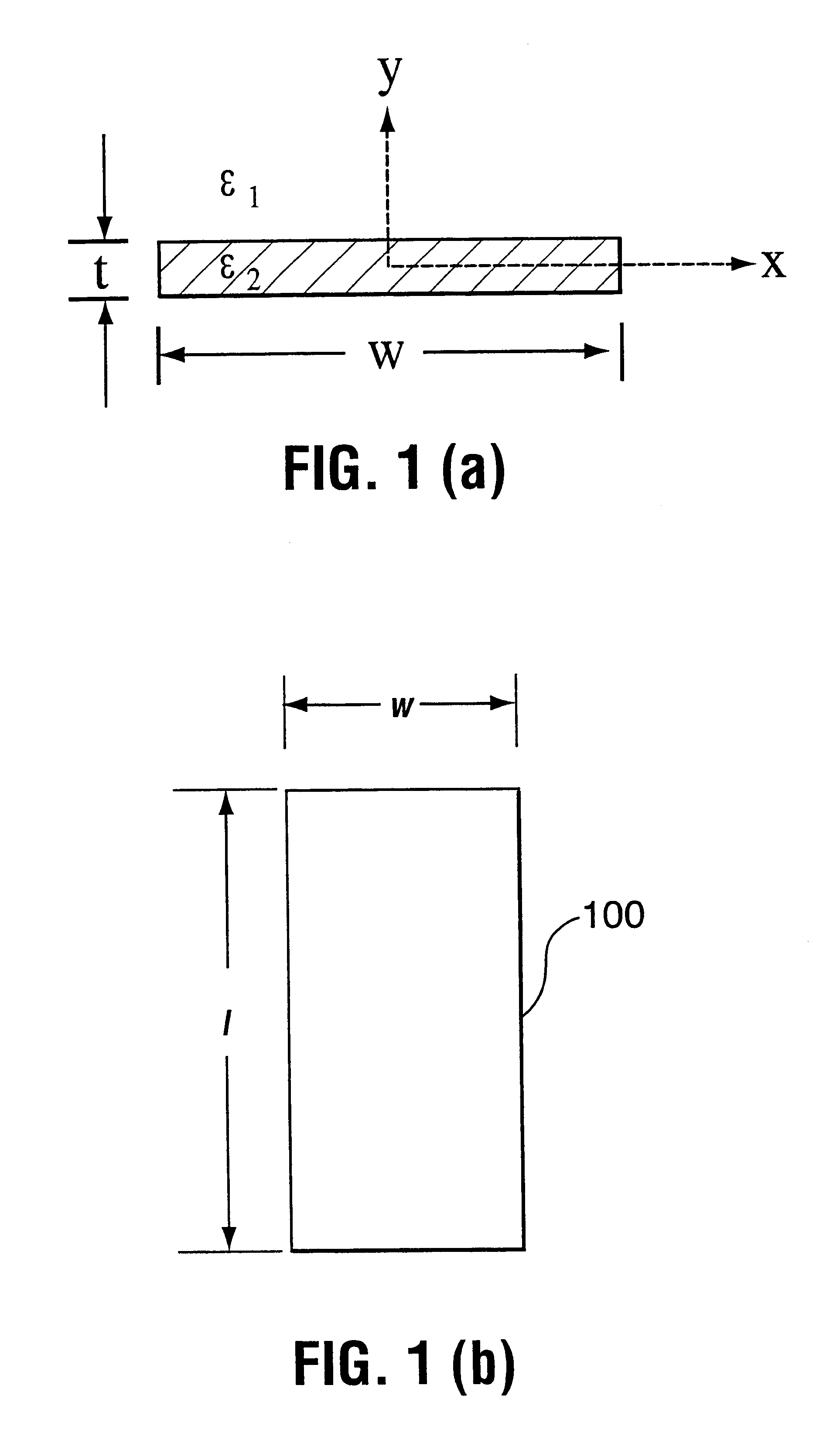
Examples of practical waveguide structures, and integrated optics devices which can be implemented using the invention, will now be described with reference also to FIGS. 27 to 42. Unless otherwise stated, where a waveguide structure is shown, it will have a general construction similar to that shown in FIGS. 1(a) and 1(b) or that shown in FIGS. 17(a) and 17(b).

The waveguide structure 100 shown in FIGS. 1(a) and 1(b) comprises a strip of finite thickness t and width w of a first material having a high free (or almost free) charge carrier density, surrounded by a second material which has a very low free carrier density. The strip material can be a metal or a highly doped semiconductor and the background material can be a dielectric.

Suitable materials for the strip include (but are not limited to) gold, silver, copper, aluminium and highly n- or p-doped GaAs, InP or Si, while suitable materials for the surrounding material include (but are not limited to) glass, quartz,...


PUM

PropertyMeasurementUnit
widthaaaaaaaaaa
free-space wavelengthaaaaaaaaaa
thickaaaaaaaaaa

Abstract

Waveguide structures comprising a thin lossy metal film of finite width embedded in an infinite homogeneous dielectric support purely bound electromagnetic modes of propagation low mode power attenuation in the neighbourhood of 10 to 0.1 dB / cm is achievable at optical communications wavelengths, with even lower values being possible. Carefully selecting the film's thickness and width can make this mode the only long-ranging one supported. In addition, the mode can have a field distribution that renders it excitable using an end-fire approach. The finite-width metal film waveguide may be used for applications requiring short propagation distances and 2-D field confinement in the transverse plane, enabling various devices to be constructed, such as couplers, splitters, modulators, interferometers, switches and periodic structures. Under certain conditions, an asymmetric structure can support a long-ranging mode having a field distribution that is suitable to excitation using an end-fire technique.

Description

1. Technical FieldThe invention relates to optical devices and is especially applicable to waveguide structures and integrated optics.2. Background ArtThis specification refers to several published articles. For convenience, the articles are cited in full in a numbered list at the end of the description and cited by number in the specification itself. The contents of these articles are incorporated herein by reference and the reader is directed to them for reference.In the context of this patent specification, the term "optical radiation" embraces electromagnetic waves having wavelengths in the infrared, visible and ultraviolet ranges.The terms "finite" and "infinite" as used herein are used by persons skilled in this art to distinguish between waveguides having "finite" widths in which the actual width is significant to the performance of the waveguide and the physics governing its operation and so-called "infinite" waveguides where the width is so great that it has no significant ...

Claims


Application Information

Patent Timeline
Patent Type & Authority Patents(United States)
IPC IPC(8): G02B6/125G02B6/122
CPCB82Y20/00G02B6/122G02B6/1225G02B6/125
Inventor BERINI, PIERRE SIMON JOSEPH
Owner UNIVERSITY OF OTTAWA
Why Eureka
Try Eureka