Method for forming p-type semiconductor film and light emitting device using the same

a technology of p-type semiconductor film and light emitting device, which is applied in the direction of polycrystalline material growth, crystal growth process, chemistry apparatus and processes, etc., can solve the problems of low resistivity of single crystal or thin film, inability to obtain p-type zno thin film, and often occur lattice mismatch, etc., to achieve easy reduction of resistance, high resistance, and large resistivity

Inactive Publication Date: 2003-09-09
MURATA MFG CO LTD
View PDF20 Cites 32 Cited by
  • Summary
  • Abstract
  • Description
  • Claims
  • Application Information

AI Technical Summary

Problems solved by technology

However, in the conventional ZnO-based group II-VI compound semiconductor, it is only possible to form a single crystal or thin film of n-type conductivity, and moreover, it is only possible to form a single crystal or thin film with low resistivity.
In such a case, however, only the n-type is produced, and even with the doping of impurities, it is not possible to obtain a p-type ZnO thin film.
Consequently, in order to obtain a pn junction using the group II-VI compound semiconductor, the group II-VI compound semiconductor must be combined with a semiconductor of a different type, and thus lattice mismatching often occurs.

Method used


Image

  • Method for forming p-type semiconductor film and light emitting device using the same
  • Method for forming p-type semiconductor film and light emitting device using the same
  • Method for forming p-type semiconductor film and light emitting device using the same

Examples


Embodiment Construction

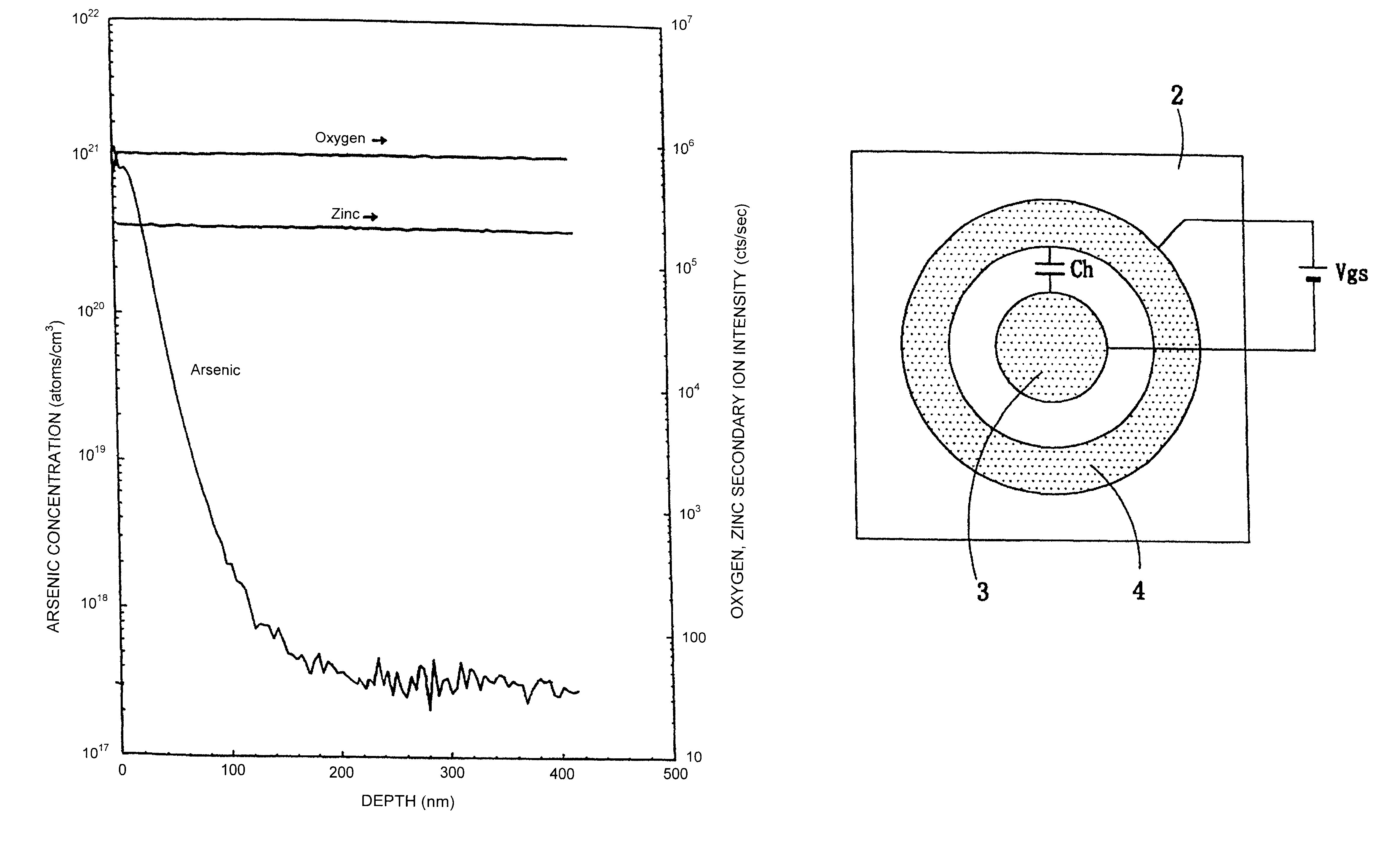
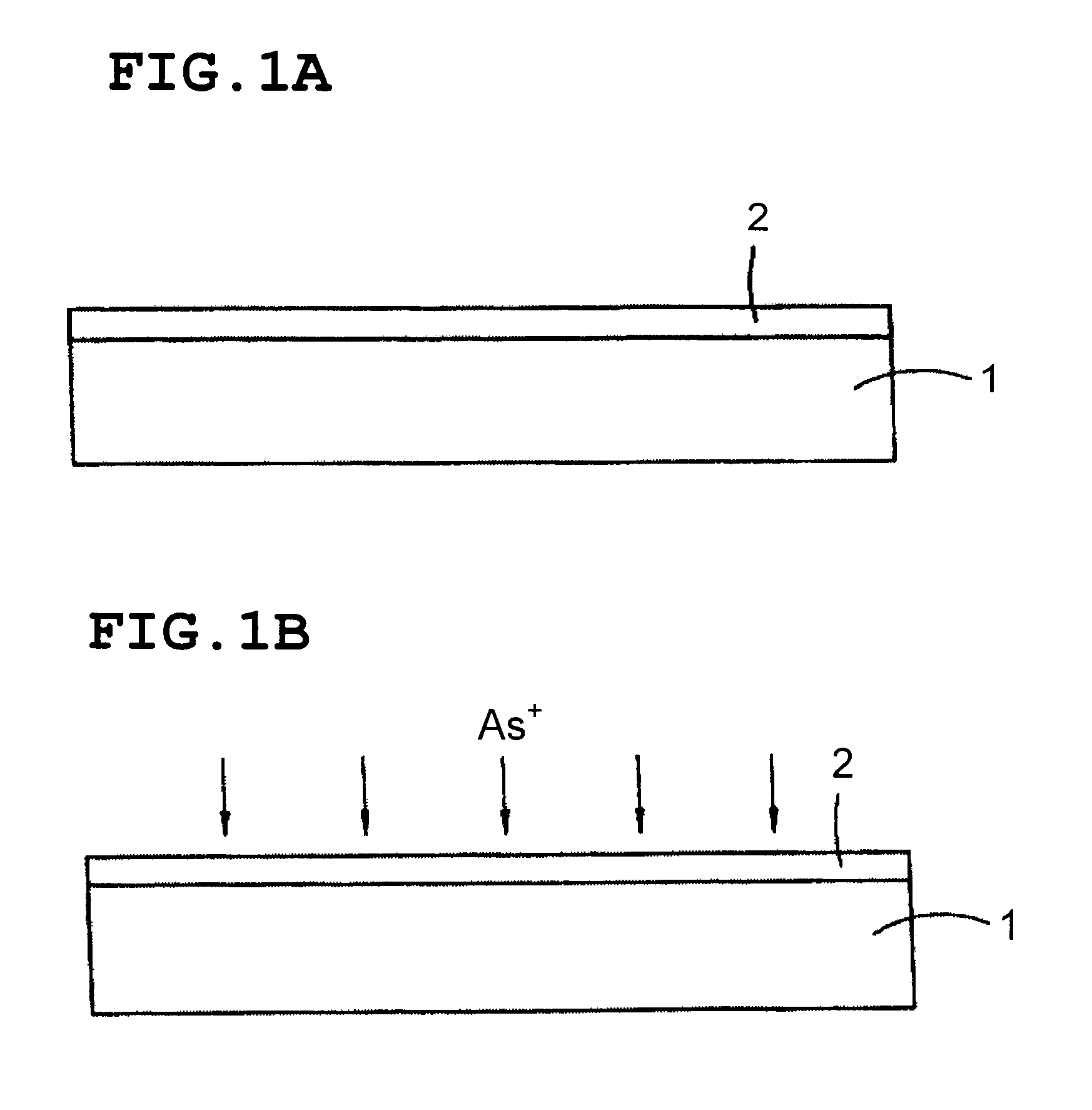
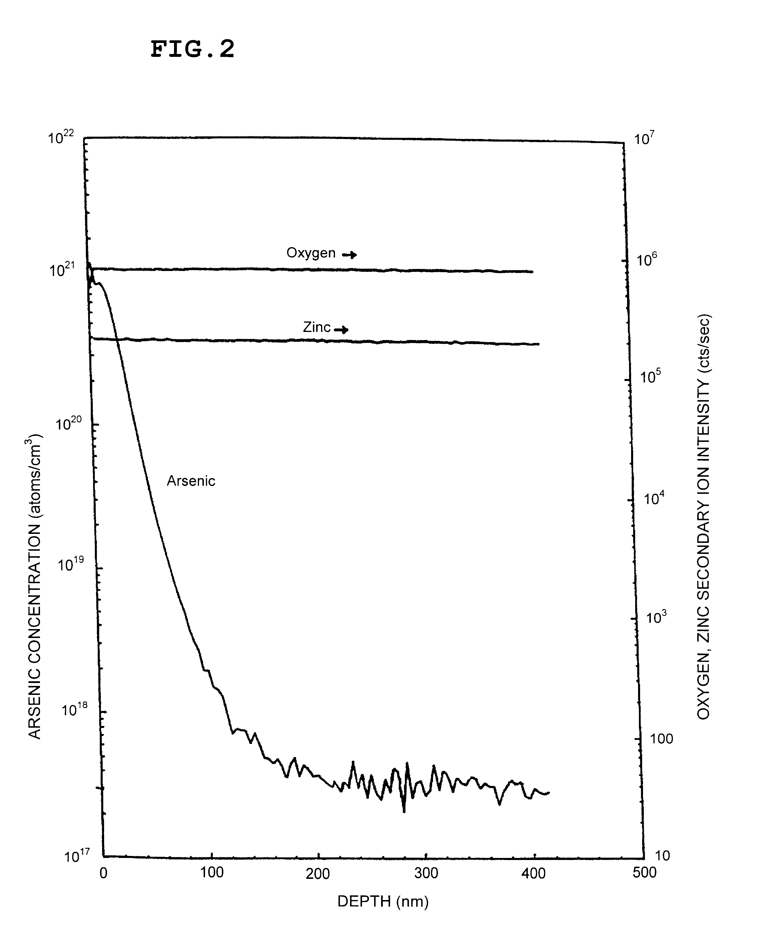
ZnO was epitaxially grown on a c-plane sapphire substrate 1 by sputtering using a Zn target with a purity of 99.9999% (6N), and thus a ZnO single-crystal thin film 2 with a thickness of 1 .mu.m was formed on the c-plane sapphire substrate 1, as shown in FIG. 1A. The ZnO thin film 2 had a resistivity .rho. of 10.sup.8 .OMEGA..multidot.cm. Next, as shown in FIG. 1B, As.sup.+ ions were implanted into the ZnO thin film 2 at an acceleration voltage of 40 kV. The doped ZnO thin film 2 had a resistivity of 10.sup.7 .OMEGA..multidot.cm. The c-plane sapphire substrate 1 provided with the ZnO thin film 2 was then annealed at 460.degree. C. for 2 hours. As a result, the resistivity was decreased to 10 .OMEGA..multidot.cm. When another ZnO thin film having a resistivity of 10.sup.6 .OMEGA..multidot.cm after deposition was subjected to ion implantation and annealing, the resistivity was decreased to 20 .OMEGA..multidot.cm.

FIG. 2 is a graph showing the As ion concentration profile, obtained by se...


PUM

PropertyMeasurementUnit
resistivityaaaaaaaaaa
temperatureaaaaaaaaaa
thicknessaaaaaaaaaa

Abstract

A method for forming a p-type semiconductor film comprises the steps of: providing on a substrate a group II-VI compound semiconductor film which is doped with a p-type impurity and comprises either MgXZn1-XO (0<=X<=1) or CdXZn1-XO (0<=X<=1) and activating the p-type impurity by annealing the doped semiconductor film.

Description

1. Field of the InventionThe present invention relates to a method for forming a compound semiconductor thin film containing a ZnO-based group II-VI compound semiconductor as a principal constituent, and to a light emitting device using the same.2. Description of the Related ArtZnO, which is a group II-VI compound semiconductor, is receiving attention as a material for light emitting devices for emitting light in the ultraviolet band, and since it is of a direct gap type, the light emission efficiency is high.In a light emitting device, such as a light emitting diode or a semiconductor laser, a pn junction comprising a p-type semiconductor layer and an n-type semiconductor layer is formed on a substrate. Accordingly, in order to fabricate a light emitting device, a p-type semiconductor layer and an n-type semiconductor layer must be grown on a substrate. When a semiconductor layer of one conductive type is epitaxially grown on a substrate and a semiconductor layer of another conduct...

Claims


Application Information

Patent Timeline
Patent Type & Authority Patents(United States)
IPC IPC(8): C30B23/02H01L33/00
CPCC30B23/02H01L21/425H01L33/0087H01L33/0095C30B29/16
Inventor KADOTA, MICHIONEGORO, YASUHIROMIURA, YOSHINORI
Owner MURATA MFG CO LTD
Why Eureka
Try Eureka