

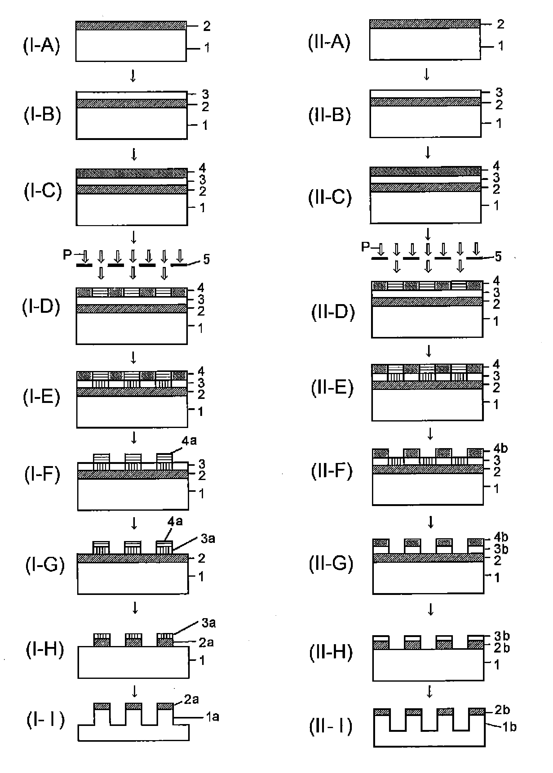
Composition for forming resist underlayer film and patterning process using the same
a technology of resist and underlayer film, applied in the direction of photomechanical equipment, coatings, instruments, etc., can solve the problems of insufficient performance of photo resist and economic irrationality, and achieve excellent adhesion, high etching selectivity, and good surface roughness
- Summary
- Abstract
- Description
- Claims
- Application Information
AI Technical Summary
Benefits of technology
Problems solved by technology
Method used
Image

Examples
examples
[0168]Although Synthesis examples, Examples, and Comparative examples will be shown and the present invention will be explained in detail hereafter, the present invention is not restricted to the following Examples. Note that the symbol “%” in the Examples represents a mass %, and the molecular weight measurement was based on GPC.
Synthesis of the Component (A)
synthesis example a-1
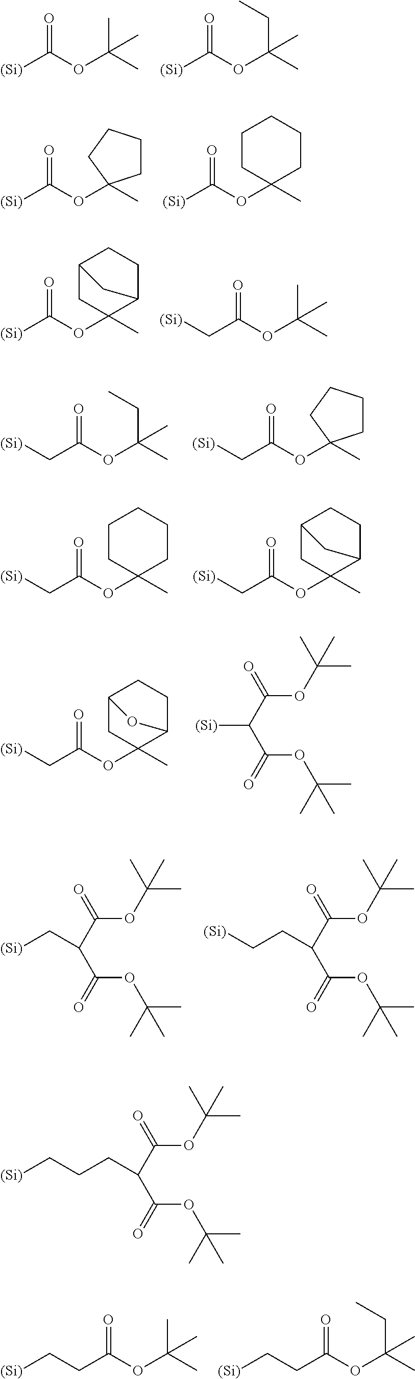
[0169]Into a mixture of 120 g of methanol, 1 g of methansulfonic acid, and 60 g of deionized water was added a mixture of 33.8 g of 4-t-butoxyphenyl trimethoxy silane (Monomer-120), 17.0 g of methyl trimethoxy silane (Monomer-101), and 47.0 g of triisopropyl borate (Monomer-110); and then, the hydrolysis-condensation reaction was carried out at 40° C. for 12 hours. After the reaction, 100 g of propylene glycol ethyl ether (PGEE) was added into it, and then, by-produced alcohols were removed by distillation under reduced pressure. Into it were added 1000 mL of ethyl acetate and 300 g of PGEE to separate an aqueous layer. Into an organic layer remained was added 100 mL of ion-exchange water; and then, the resulting mixture was agitated, settled, and separated into the layers. This procedure was repeated for three times. The organic layer remained was concentrated under reduced pressure to obtain 300 g of PGEE solution of the silicon-containing compound A-1 (polymer concentration of 15...
synthesis example a-21
[0171]Into a mixture of 240 g of ethanol, 6 g of 25% tetramethylammonium hydroxide, and 120 g of deionized water was added a mixture of 67.6 g of 4-t-butoxyphenyl trimethoxy silane (Monomer-120), 17.0 g of methyl trimethoxy silane (Monomer-101), 5.0 g of phenyl trimethoxy silane (Monomer-100), and 18.8 g of triisopropyl borate (Monomer-110); and then, the hydrolysis-condensation reaction was carried out at 40° C. for 4 hours. After the reaction, 10 g of acetic acid was added into it for neutralization, and then, by-produced alcohols were removed by distillation under reduced pressure. Into it were added 1000 mL of ethyl acetate and 300 g of PGEE to separate an aqueous layer. Into an organic layer remained was added 100 mL of ion-exchange water; and then, the resulting mixture was agitated, settled, and separated into the layers. This procedure was repeated for three times. The organic layer remained was concentrated under reduced pressure to obtain 300 g of PGEE solution of the sili...
PUM
| Property | Measurement | Unit |
|---|---|---|
| contact angle | aaaaa | aaaaa |
| contact angle | aaaaa | aaaaa |
| wavelength | aaaaa | aaaaa |
Abstract
Description
Claims
Application Information