Low frequency electromagnetic absorption surface

a technology of electromagnetic absorption and low frequency, applied in the direction of magnetic/electric field screening, electrical equipment, and space probes, etc., can solve the problems of complex profiles that cannot be easily made on metal layers, plasmons cannot be converted back to photons for re-emission, and are far heavier than electric absorbers. , to achieve the effect of simple fabrication

Inactive Publication Date: 2003-11-04
QINETIQ LTD
View PDF11 Cites 20 Cited by
  • Summary
  • Abstract
  • Description
  • Claims
  • Application Information

AI Technical Summary

Benefits of technology

to provide for a relatively thin, lightweight, broadband absorber, which is relatively simple to fabricate and incorporates a second damping mechanism by which the SPP may decay.

Problems solved by technology

The energy is absorbed by the metal due to damping of the charge density oscillation (i.e. charge collisions lead to heating in the metal), and hence the plasmons cannot convert back to photons for re-emission.
In the case of magnetic absorbers these are placed directly onto the metal plate. but they are far heavier than electric absorbers.
The disadvantage is that complicated profiles cannot easily be made on a metal layer and expensive and complicated techniques of machining metal are required.
In addition, the SPP that propagates along the textured surface may only be radiatively damped since the media either side of the boundary are usually non-absorbing.
Secondly, although the top and bottom semi-infinite media (air and metal respectively) are effectively non-absorbing, at these frequencies, this may not be true for dielectrics, such as wax.

Method used


Image

  • Low frequency electromagnetic absorption surface
  • Low frequency electromagnetic absorption surface
  • Low frequency electromagnetic absorption surface

Examples


Embodiment Construction

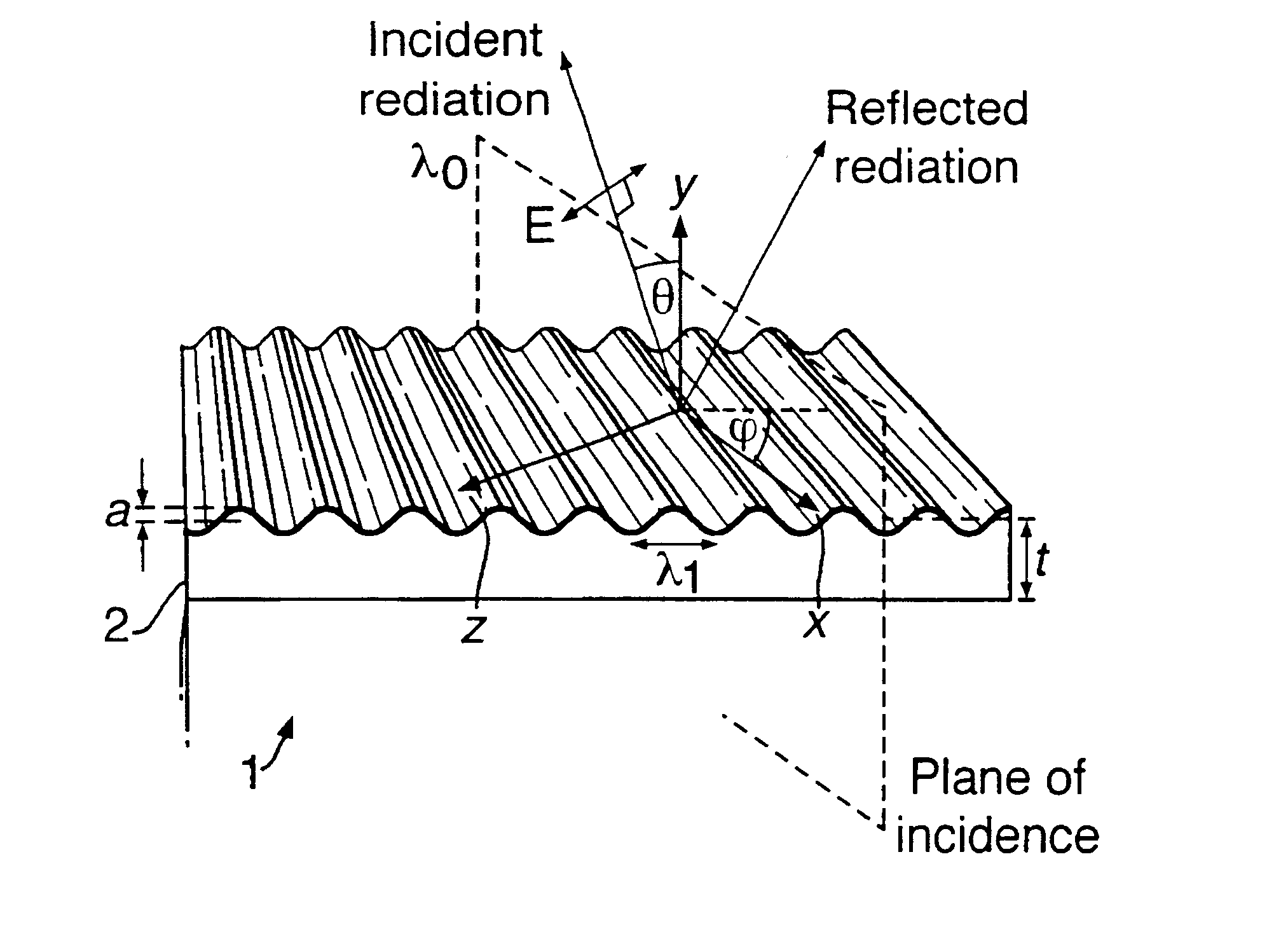
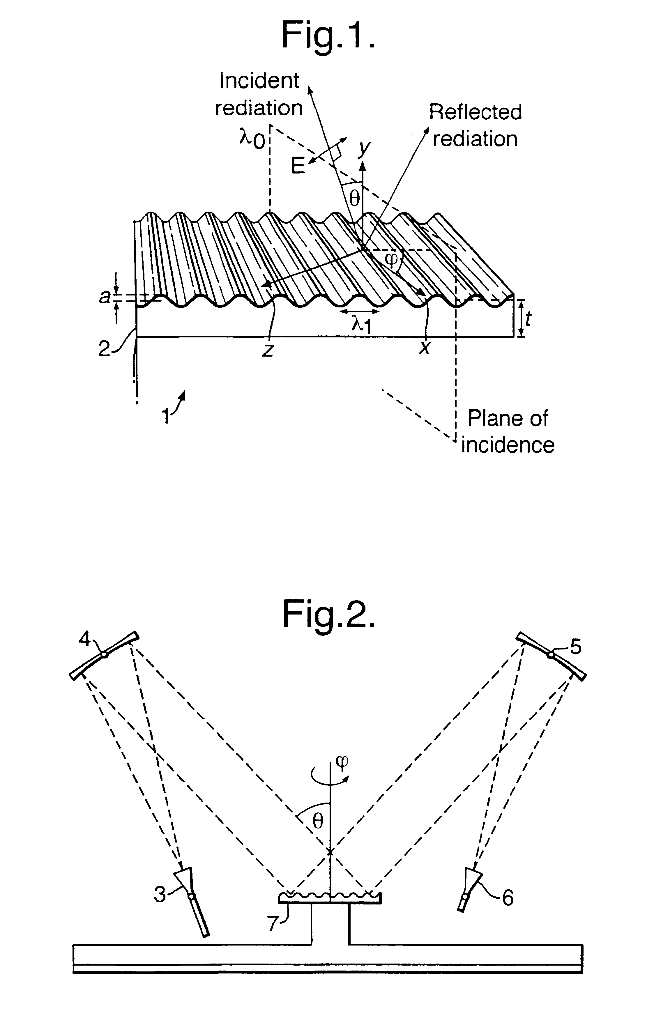
FIG. 1 shows the substrate 1 having a dielectric layer of petroleum wax 2 with a profiled surface. This profile is corrugated (sinusoidal) and having pitch p, amplitude a, and dielectric thickness t. The sinusoidal top interface profile A(x)=a cos 2.PI.x / .lambda.g, where t.apprxeq.2.6 mm, a .apprxeq.1.5 mm and .lambda.g.apprxeq.15 mm.

The sample is prepared by filling a metallic, square tray of side approximately 400 mm and depth 5 mm with hot wax and allowing it to cool. A metallic "comb" of the desired sinusoidal interface profile is manufactured using a computer-aided design and manufacture technique. It is used to remove unwanted wax from the sample by carefully dragging it across the surface until the required grating profile is obtained.

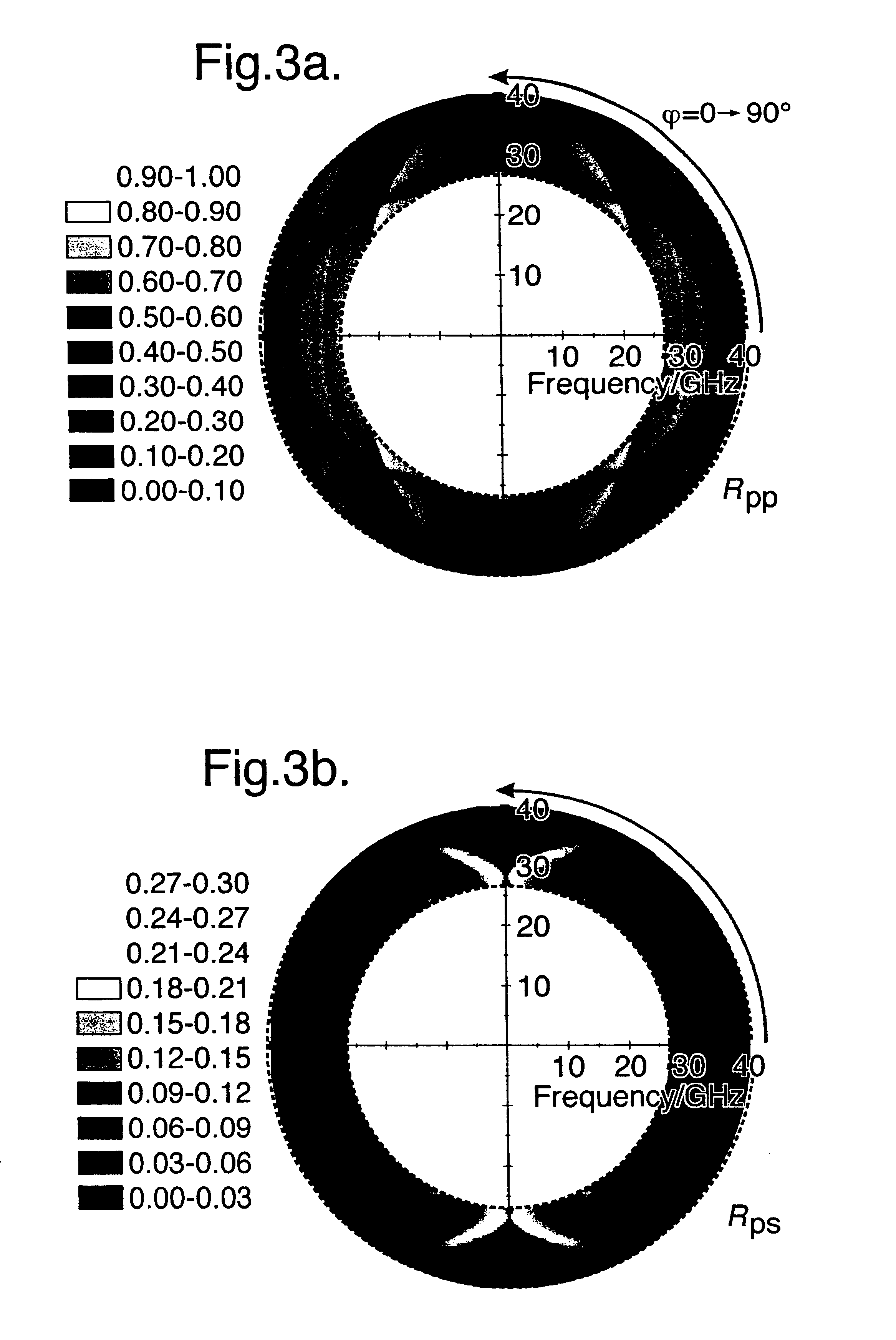
FIG. 2 shows an arrangement used to record reflectivity from the sample. A transmitting horn 3 is placed at the focus of a 2 m focal length mirror 4 to collimate the beam therefrom. A second mirror 5 is positioned to collect the specularly refle...


PUM


Abstract

A radiation absorber comprising a substrate having free charges capable of being driven to form resonance charge density oscillators and a dielectric layer coated onto said surface wherein the dielectric layer has a textured/patterned surface. The substrate is preferably metallic and the dielectric layer is waveform.

Description

1. Field of the InventionThe invention relates to low-frequency electromagnetic absorption surfaces.2. Discussion of Prior ArtSurface plasmon polaritons (SPPs) are charge density oscillations induced at the surface of a metal at a metal-dielectric interface when photons are coupled to the mode in the correct manner. The momentum of the incident photons must be boosted if the resonant condition is to be met, and this can be achieved by corrugating the metal to form a diffraction grating. The energy is absorbed by the metal due to damping of the charge density oscillation (i.e. charge collisions lead to heating in the metal), and hence the plasmons cannot convert back to photons for re-emission. In this manner the reflectivity of the metal is reduced when photons are absorbed. This phenomenon is well known at visible frequencies, and forms the basis of many sensor designs.At microwave frequencies any SPPs that are excited at the surface of the metal will propagate without loss because...

Claims


Application Information

Patent Timeline
Patent Type & Authority Patents(United States)
IPC IPC(8): H01Q17/00H05K9/00
CPCH01Q17/00H01Q17/008H01Q17/007
Inventor LAWRENCE, CHRISTOPHER RSAMBLES, JOHN RHIBBINS, ALISTAIR P
Owner QINETIQ LTD
Why Eureka
Try Eureka