

Self-aligned silicide process for silicon sidewall source and drain contacts
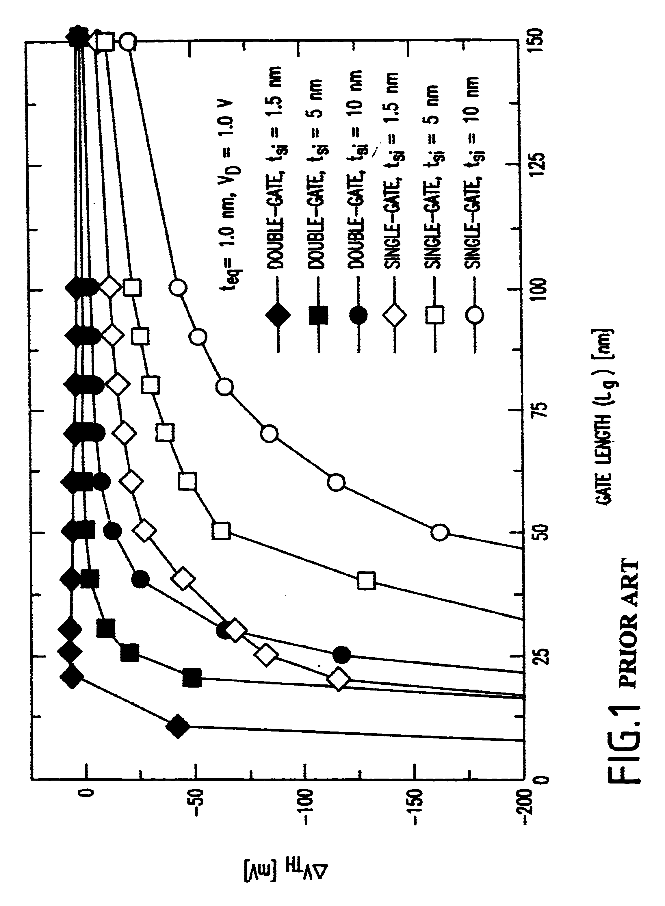
a silicon sidewall source and drain contact technology, applied in the direction of transistors, semiconductor devices, electrical equipment, etc., can solve the problems of large difference in the threshold voltage (vt) of devices across the wafer, circuit failure, and possible problems
- Summary
- Abstract
- Description
- Claims
- Application Information
AI Technical Summary
Benefits of technology
Problems solved by technology
Method used
Image

Examples
Embodiment Construction
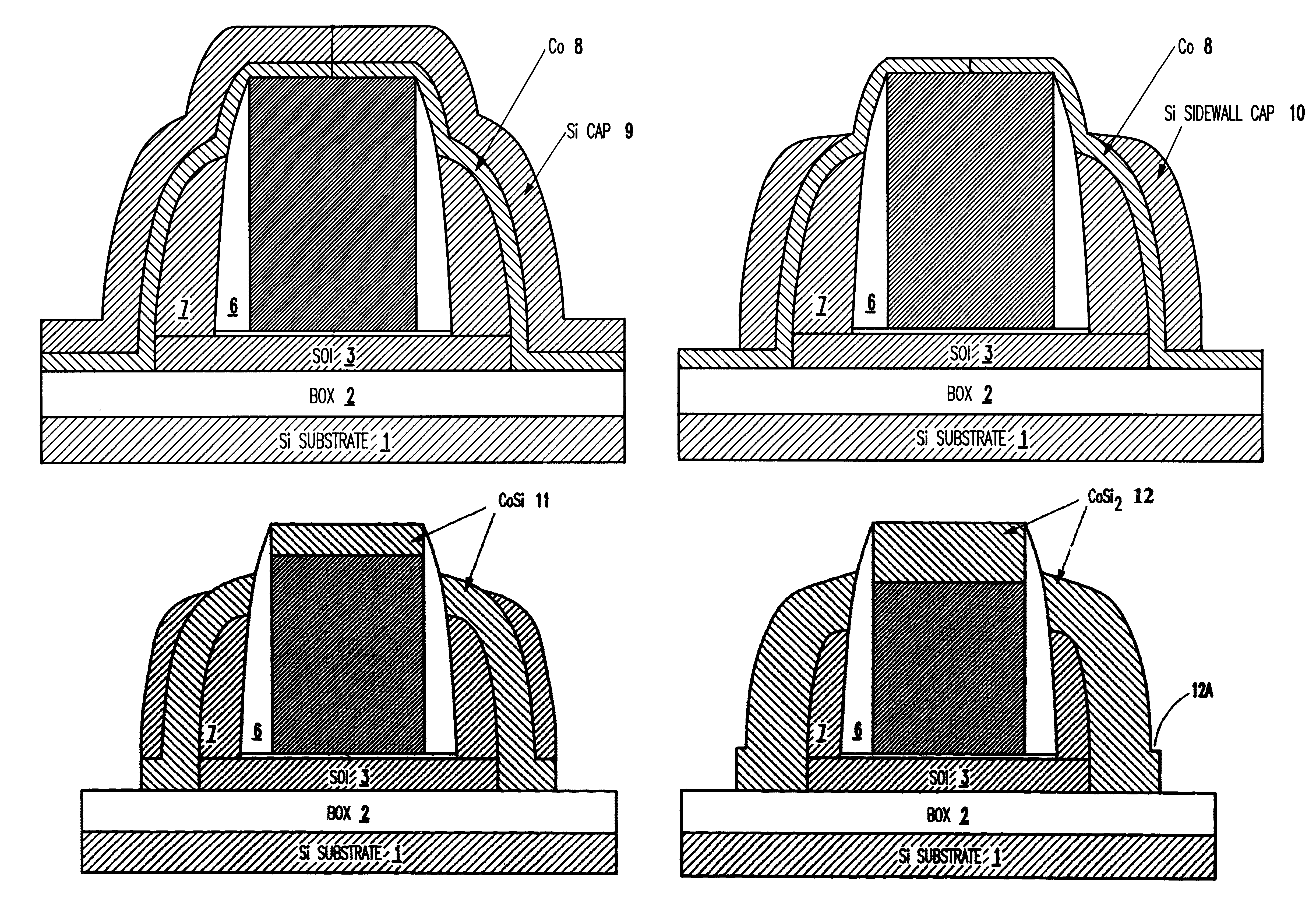
Turning now to FIGS. 2B and 5-11B, preferred embodiment of the present invention will be described hereinafter.
However, prior to discussing the present invention in detail, it is noted that, for the sake of simplicity only and not for limiting the scope of the invention in any way, the method discussed below is for the specific case of Cobalt (Co) silicide. Cobalt has been used because it provides a lowest resistivity silicide. Thus, although Co silicide is of a special interest due to its superior properties, the method is general and applicable to silicides formed with other metals such as Ti, Pt, Ni, Pd, W etc.
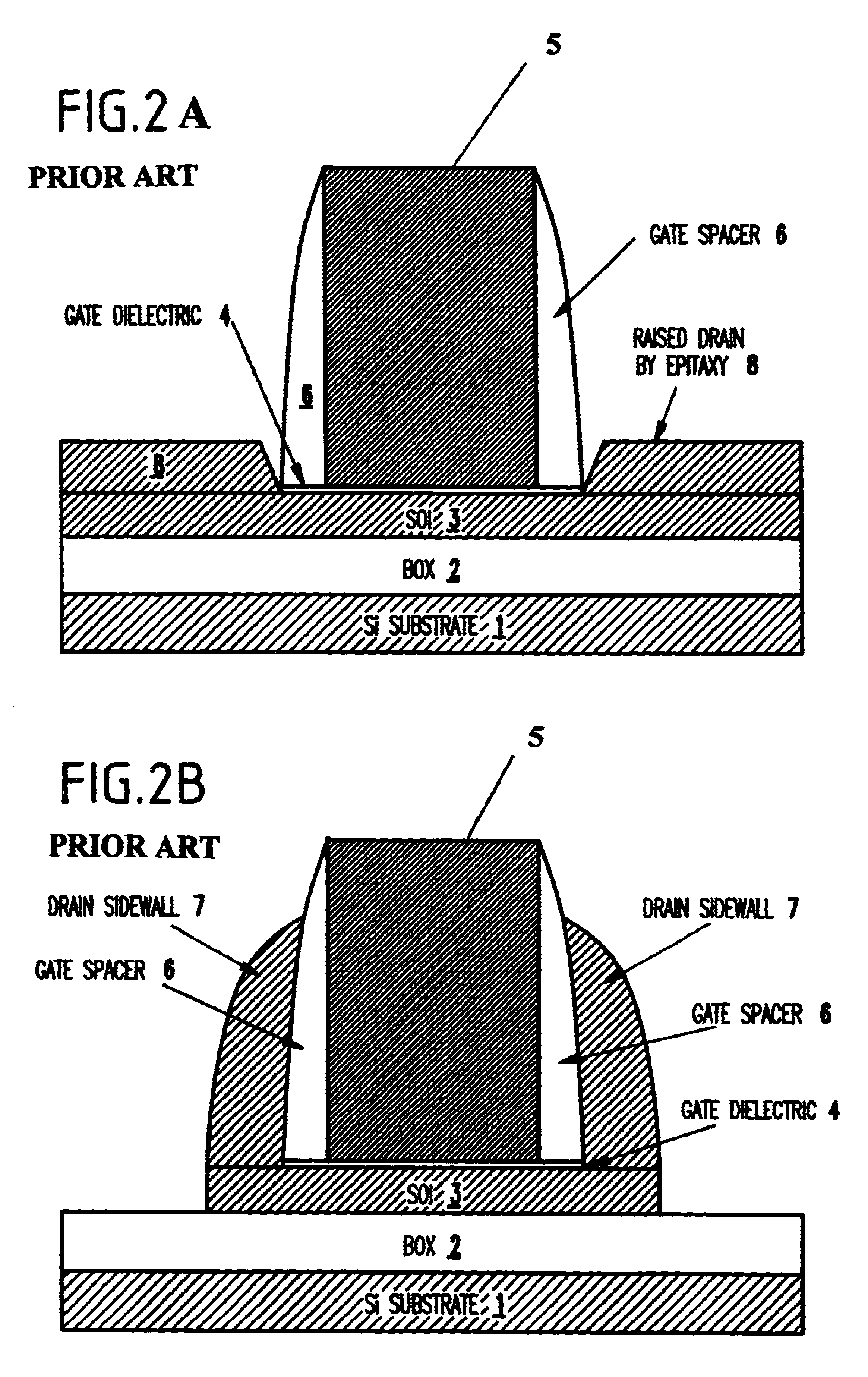
Turning now to the drawings, FIG. 2B shows an initial device to be silicided. The structure includes a Si substrate 1, a buried oxide (BOX) layer 2, a silicon-on-insulator (SOI) film 3, a gate dielectric 4, a patterned gate 5, two sidewall spacers 6, and the silicon sidewall source and drain 7. The silicon sidewalls are heavily doped and may be considered as source and drai...
PUM
| Property | Measurement | Unit |
|---|---|---|
| thickness | aaaaa | aaaaa |
| thickness | aaaaa | aaaaa |
| temperature | aaaaa | aaaaa |
Abstract
Description
Claims
Application Information