Offset correction and slicing level adjustment for amplifier circuits

Inactive Publication Date: 2003-12-02
SKYWORKS SOLUTIONS INC
View PDF7 Cites 75 Cited by
  • Summary
  • Abstract
  • Description
  • Claims
  • Application Information

AI Technical Summary

Problems solved by technology

Implementation of a high-speed AGC amplifier in a CMOS process presents many challenges.
One reason for this is that a high quality diode is not readily available in a standard CMOS process.
Though a similar function can be implemented using MOS devices, the circuit non-idealities and limited bandwidth of the devices make amplitude detection difficult.
An undesired offset in the amplifier can prevent the proper detection of small signals and random amplifier offsets, due to mismatch between critical devices, become greater with smaller device sizes.
Many existing offset correction systems employ a purely analog approach, which makes realization of this low bandwidth only possible with large external passive devices.
That results in extra pins on the integrated circuit being devoted to connecting these passive devices.
However, the available number of pins can be limited on integrated circuits such as those implementing clock and data recovery circuits, and extra pins can result in bigger packages and thus bigger component costs.
Not only do passive devices cost both board area and adversely affect component cost, their use brings a very sensitive node out

Method used


Image

  • Offset correction and slicing level adjustment for amplifier circuits
  • Offset correction and slicing level adjustment for amplifier circuits
  • Offset correction and slicing level adjustment for amplifier circuits

Examples


Embodiment Construction

)

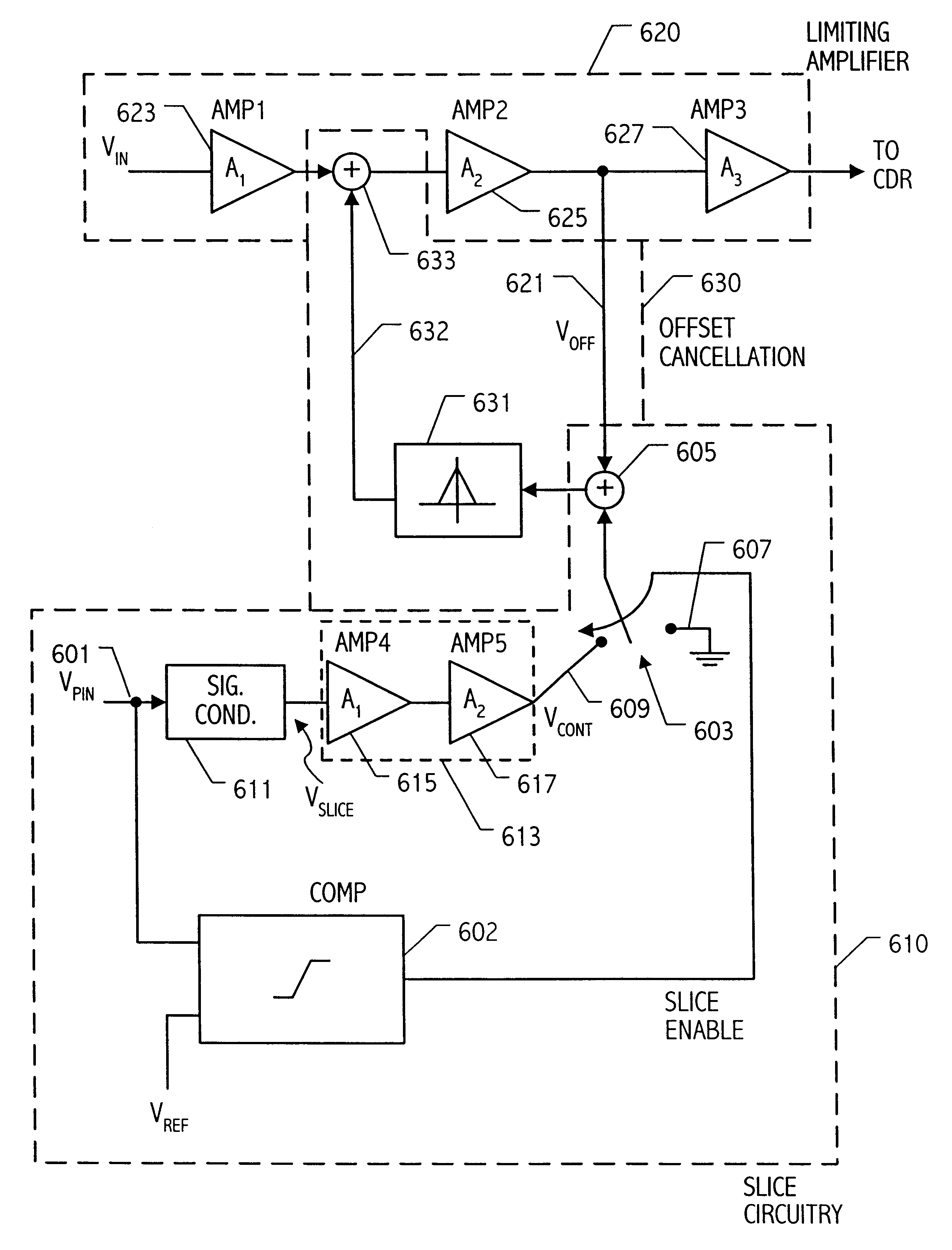
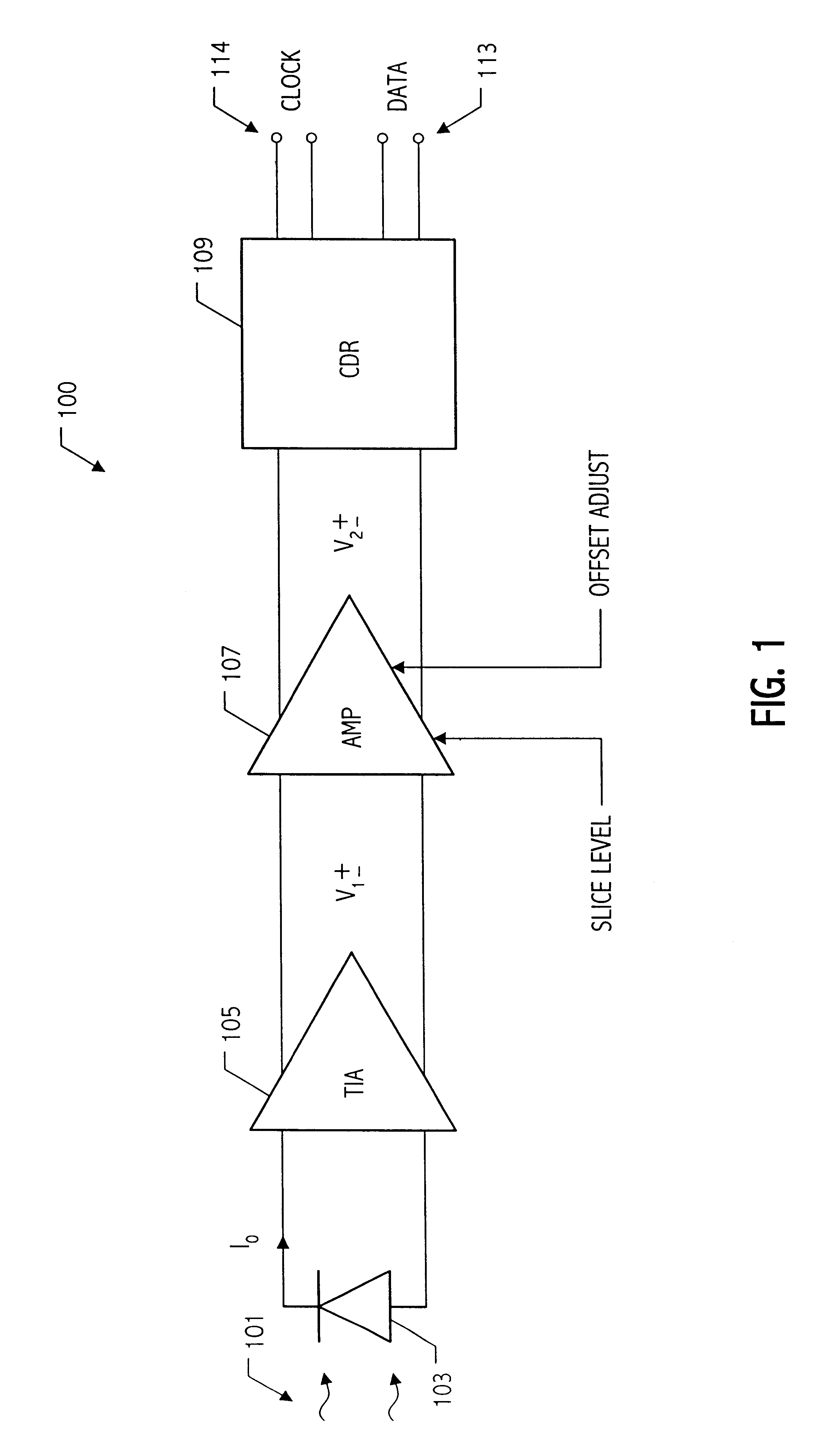
Referring to FIG. 6, a block-level diagram illustrates a slice and offset correction circuit that achieves slice adjustment and offset correction without the offset correction canceling the slice adjustment. The illustrated embodiment includes a slice circuit 610, an amplifier 620, and an offset correction circuit 630. In a preferred embodiment the amplifier is a multi-stage limit amplifier implemented in CMOS. Because CMOS circuits can recover quickly from an overdrive condition, a limit amplifier is well suited for CMOS. The amplifier 620 includes amplifier stage 623 (AMP1), amplifier stage 625 (AMP2) and amplifier stage 627 (AMP3). Amplifier stage 627 represents one or more stages. In one embodiment, there are six amplifier stages.

The slice level is provided at input pin 601, which in the illustrated embodiment, is the only pin required to implement slicing and offset control. In other embodiments, the slice level may be provided by other communications paths to the slice circui...


PUM


Abstract

A slice and offset circuit is provided that uses a digital integrator in the feedback loop of the offset cancellation circuitry. A slice circuit receives an indication of a desired slice voltage and supplies a signal to specify the slice level, which is combined with a sensed offset level of the amplifier. The feedback loop includes a low pass filter that receives the combined signal indicative of the offset and the slice level. The low pass filter includes the digital integrator circuit that includes an up/down counter that counts in a direction determined according to a digital signal having a ones-density indicative of a value of the combined signal with respect to a reference signal, thereby generating a feedback signal that cancels offset and adjusts for slice.

Description

1. Field of the InventionThis invention relates to amplifier circuits and more particular to offsets associated with amplifiers.2. Description of the Related ArtFIG. 1 shows the block diagram of a typical high-speed optical receiver 100, designed to work at rates of, e.g., 2.7 GHz. The received optical energy 101 is converted to a current using a photodiode, 103. The photodiode signal current I.sub.o is converted to a voltage using the transimpedance amplifier (TIA) 105. The signal at the output of TIA 105 is small for low optical energy signals, and can contain significant corruption due to, e.g., noise and limited rise and fall times. The typical range of signal amplitude at the output of the TIA 105 is from a few millivolts to a few hundred millivolts. TIA 105 is followed by additional gain, usually implemented with a limit amplifier or an automatic gain control (AGC) amplifier 107. Note that although FIG. 1 shows a fully differential system, it is common for some of the illustra...

Claims


Application Information

Patent Timeline
IPC IPC(8): H03F3/08H03F3/45H03F3/04H03L7/06
CPCH03F3/087H03F3/45973H03L7/06H03F2200/331
Inventor KING, ERIC T.PERROTT, MICHAEL H.PASTORELLO, DOUGLAS F.
Owner SKYWORKS SOLUTIONS INC
Why Eureka
Try Eureka