Separation method of semiconductor layer and production method of solar cell

a production method and technology of solar cells, applied in the field of separation of semiconductor layers and production methods of solar cells, can solve the problems of difficult to completely remove adhesives, chipping and cracking of wafers, and polluting the global environmen

Inactive Publication Date: 2004-01-27
CANON KK
View PDF9 Cites 156 Cited by
  • Summary
  • Abstract
  • Description
  • Claims
  • Application Information

AI Technical Summary

Problems solved by technology

The greenhouse effect gases, e.g., carbon dioxide and nitrogen oxides resulting from burning oil at thermal power plants and gasoline by vehicles, are polluting the global environments.
In this method, since the wafer was diced with a low-elasticity dicing tape attached to its back side, strain was generated in the wafer during the dicing step, thereby leading to chipping and cracking of the wafer.
In other words, it is difficult to completely remove the adhesive 109 from the Si wafer 101, and the Si wafer may be damaged during the removal step.
A porous layer used as the separation layer is required (1) to be easily separated, i.e., to have a fragile structure, and (2) to stabl

Method used


Image

  • Separation method of semiconductor layer and production method of solar cell
  • Separation method of semiconductor layer and production method of solar cell
  • Separation method of semiconductor layer and production method of solar cell

Examples


embodiment 1

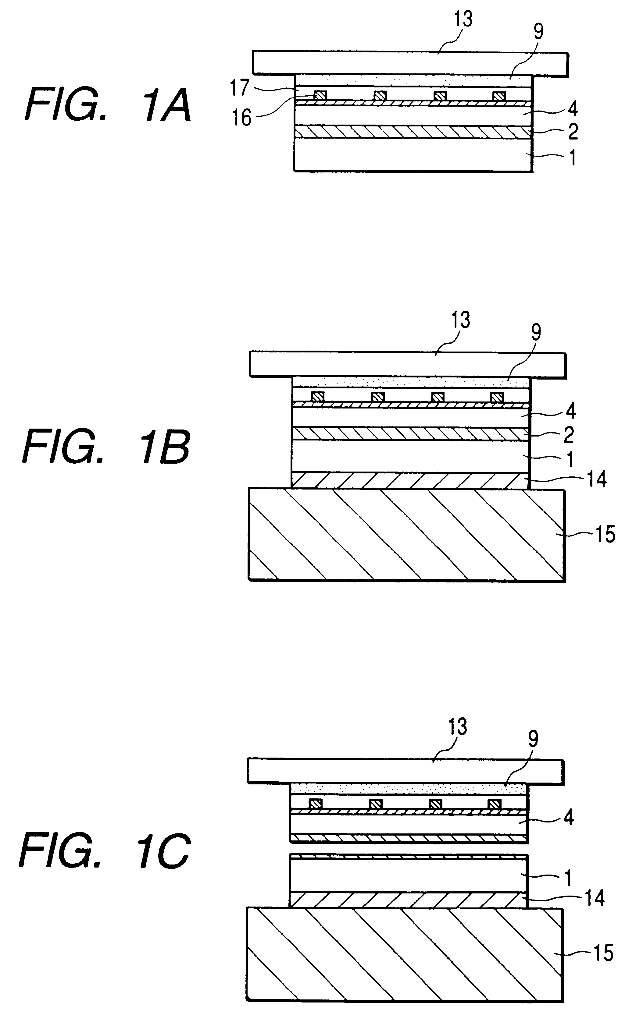
Embodiment 1 will be described the production steps of a solar cell, which is obtained by forming a porous Si layer on a Si wafer by anodization; depositing single-crystal Si layers on the porous Si layer by an apparatus for liquid-phase growth; forming grid electrodes; and peeling off the single-crystal Si layers, and which has a structure that the single-crystal Si layers of the solar cell produced are irradiated with light from the surface side on which the epitaxial growth of the Si layer is stopped (grid electrode side).

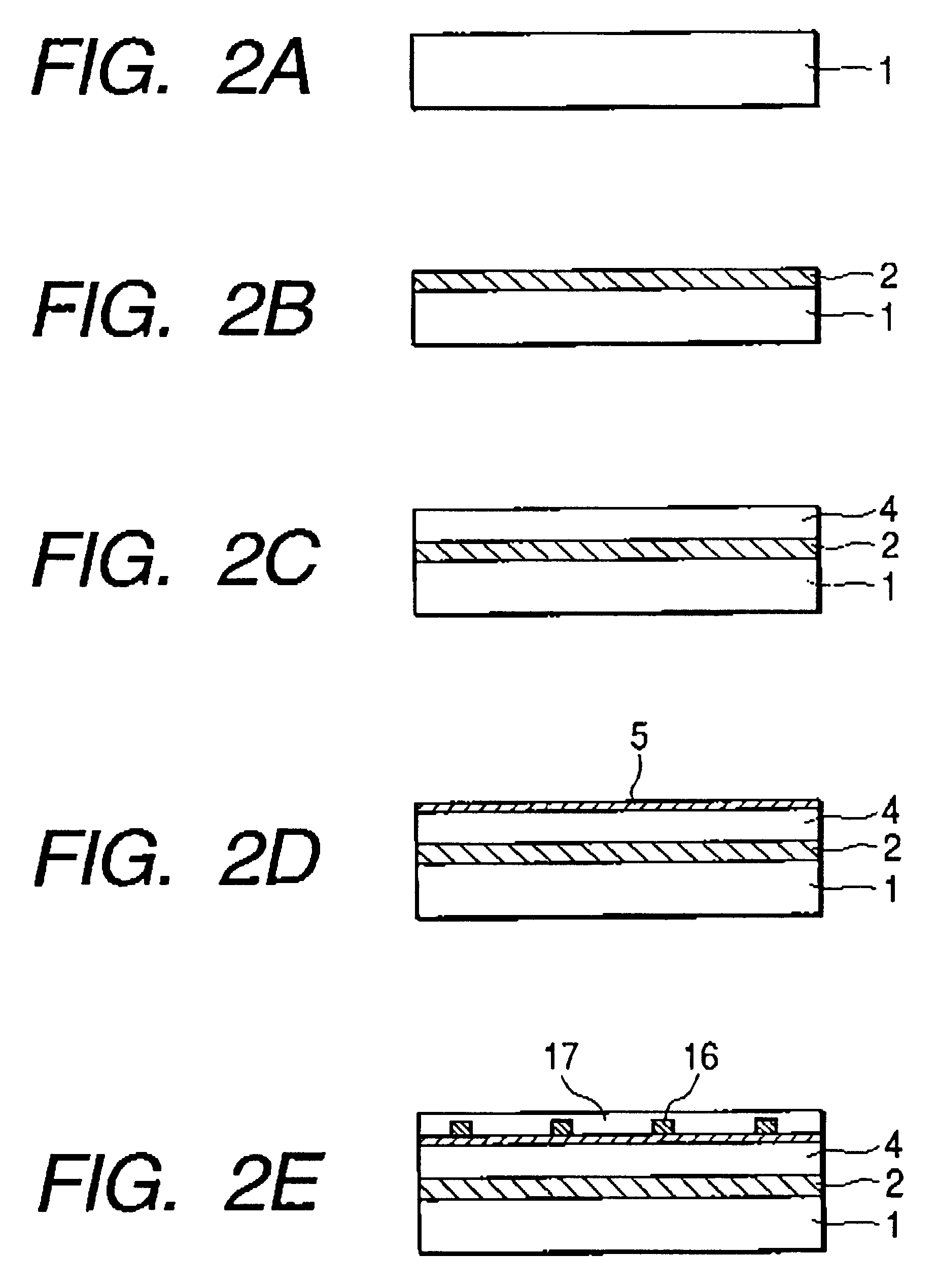
FIGS. 1A to 1C through 3A to 3C show the schematic sections illustrating the production steps of the production method of a thin-film single-crystal Si solar cell according to Embodiment 1 of the present invention. First, the Si wafer 1 is prepared (FIG. 2A). Then, the Si wafer 1 is anodized to form the porous Si layer 2 thereon (FIG. 2B). FIGS. 18A and 18B show the sections illustrating apparatuses for anodizing the Si wafer 1 in a hydrofluoric acid-based etcha...

embodiment 2

Embodiment 2 will be described the production steps of a solar cell, the solar cell produced being irradiated with light from the single-crystal Si layer on the surface side on which the epitaxial growth of the Si layer is stopped (grid electrode side). FIGS. 4A to 4F through 5A to 5E show the schematic sections illustrating the production steps of Embodiment 2.

The p.sup.+ type Si wafer 1 (FIG. 4A) was anodized with a solution obtained by adding isopropyl alcohol to hydrofluoric acid at 1 / 10 vol. % to form a 5 .mu.m thick porous Si layer 2 (FIG. 4B) thereon. The Si wafer 1 was set in the load lock chamber in the apparatus for liquid-phase growth. The load lock chamber was evacuated under a vacuum and filled with a hydrogen gas. Then, the gate valve leading to the growth chamber was opened, to transport the substrate into the growth chamber. It was annealed at about 1050.degree. C., cooled to 950.degree. C., and dipped in the indium solvent supersaturated beforehand with Si. The solv...

embodiment 3

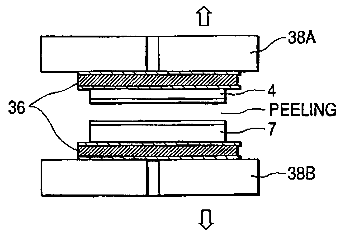
Embodiment 3 will be described production of a solar cell module with 3 solar cells (unit cell) connected in series, for which the production method of a solar cell of Embodiment 2 is efficiently used. FIGS. 6A to 6C through 9 illustrate production steps for a solar cell module of Embodiment 3, FIG. 6A showing a schematic plan and the others schematic sectional views.

In Embodiment 3, openings were provided on a part of the grid electrode 16 in the step for forming the antireflection layer 17 (FIG. 4E for Embodiment 2). The electroconductive busbar 23 (e.g., nickel-plated copper tape) was adhered to the grid electrode 16 at the openings using an electroconductive adhesive (not shown), and sintered (FIG. 6A, and FIG. 6B as the sectional view thereof). Water was sprayed over the surface of the holding substrate 30A as the holding means kept at 5.degree. C., to form a thin water layer thereon. The 3 unit cells thus prepared, kept at 5.degree. C., were arranged on the holding substrate 3...


PUM


Abstract

The separation method of a semiconductor layer according to the present invention comprises separating a semiconductor layer and a semiconductor substrate at a separation layer formed therebetween, wherein a face of the semiconductor layer at the side opposite to the separation layer and/or a face of the semiconductor substrate at the side opposite to the separation layer are held by utilizing an ice layer, whereby it is unnecessary to use an adhesive as holding means and at the same time it is possible to easily and uniformly separate them.

Description

1. Field of the InventionThis invention relates to a separation method of a semiconductor layer, and a production method of a solar cell using the semiconductor layer separated by the above separation method.2. Related Background ArtThe greenhouse effect gases, e.g., carbon dioxide and nitrogen oxides resulting from burning oil at thermal power plants and gasoline by vehicles, are polluting the global environments. Therefore, power generation by solar cells has been increasingly attracting attention, viewed from the above environmental concerns and anticipated depletion of crude oil.The solar cell of thin-film crystal silicon (Si) has various advantages; it can be produced at low cost, because of its thin power generation layer which decreases required quantity of a Si raw material, the power generating layer of crystal Si can exhibit a higher conversion efficiency and durability than the other types of solar cells, e.g., that using amorphous Si, and it can be bent to some extent, w...

Claims


Application Information

Patent Timeline
IPC IPC(8): H01L21/30H01L21/02H01L31/18H01L31/04H01L21/00H01L21/3063H01L21/68H01L21/762
CPCH01L21/67207H01L21/6835H01L21/76259H01L31/1804H01L31/0504H01L31/1892H01L2221/68368Y10S438/977Y10S438/96Y02E10/547Y02P70/50
Inventor IWANE, MASAAKINAKAGAWA, KATSUMIIWAKAMI, MAKOTONISHIDA, SHOJIUKIYO, NORITAKAIWASAKI, YUKIKOMIZUTANI, MASAKI
Owner CANON KK
Why Eureka
Try Eureka