Method for manufacturing a metal-insulator-metal capacitor

a technology of metal-insulator metal and capacitor, which is applied in the manufacture of capacitors, fixed capacitor details, stacked capacitors, etc., can solve the problems of difficult, if not impossible, to remove hard metallic polymers, interconnect lines interfering with each other,

Inactive Publication Date: 2004-03-02
SAMSUNG ELECTRONICS CO LTD
View PDF1 Cites 21 Cited by
  • Summary
  • Abstract
  • Description
  • Claims
  • Application Information

AI Technical Summary

Problems solved by technology

When the interconnection lines are closely disposed, the interconnect lines interfere with each other.
If the interval between the interconnection lines falls below a predetermined value, the entire signal is delay because of the interference between the interconnection lines.
It is difficult, if not impossible, to remove the hard metallic polymer by using an ashing process

Method used


Image

  • Method for manufacturing a metal-insulator-metal capacitor
  • Method for manufacturing a metal-insulator-metal capacitor
  • Method for manufacturing a metal-insulator-metal capacitor

Examples


Embodiment Construction

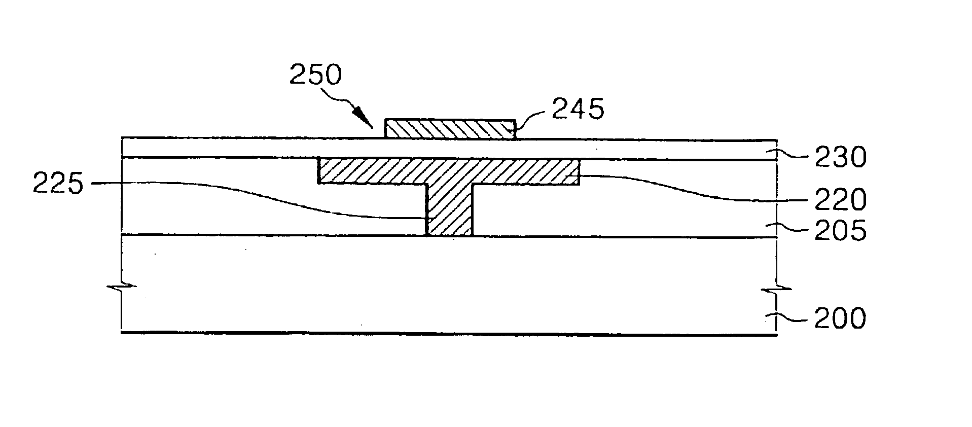
FIGS. 3A to 3E are cross-sectional views illustrating a method of manufacturing a MIM capacitor according to a preferred embodiment of the present invention.

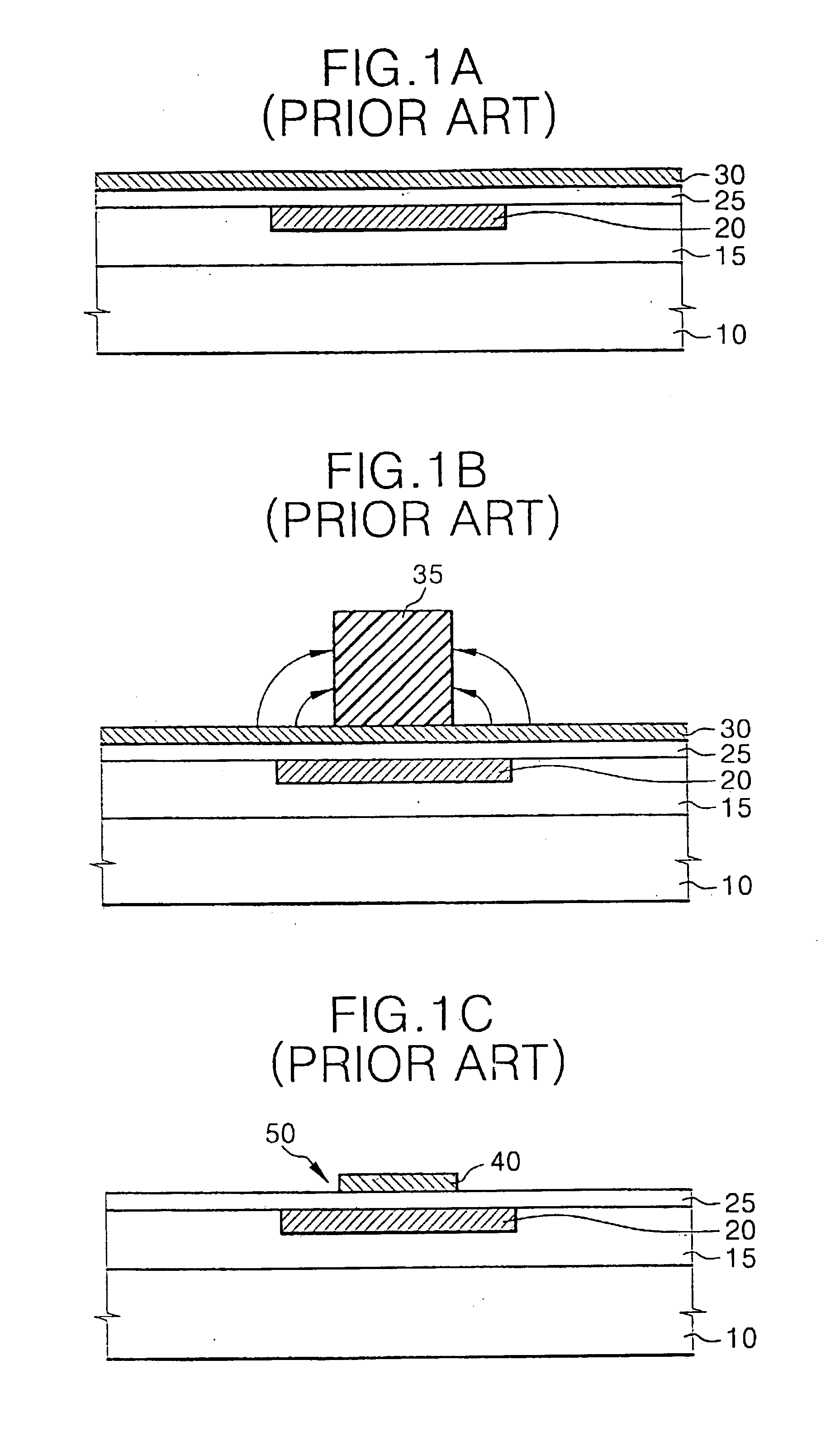
Referring to FIG. 3A, after an insulation film 105 is formed on a semiconductor substrate 100, a groove or a trench having a predetermined shape and dimension is formed in the insulation film 105 by patterning the insulation film 105. The insulation film 105 may include tetraethylortho silicate (TEOS), low temperature tetraethylortho silicate (LT-TEOS), plasma enhanced tetraethyloxysilane (PE-TEOS), or borophosphosilicate glass (BPSG).

Subsequently, a metal wire 110 is formed in the trench or the groove by employing a damascene process. That is, after the trench or the groove is formed in the insulation film 105, the trench or the groove is filled with copper (Cu) using a sputtering process, a chemical vapor deposition process, or an electro plating process. The copper film is then polished using a chemical-mechanical polishing (...


PUM


Abstract

A method of manufacturing a MIM capacitor having a bottom electrode is provided by forming a metal wire including copper on a substrate. After the metal wire is formed on the substrate, a dielectric film is formed on the metal wire. A top electrode film is formed on the dielectric film, and then the top electrode film is etched to form a top electrode. A hard metallic polymer formed during the etching of the top electrode film is removed using a mixture of an oxygen gas and a fluorocarbon based gas. The lifting of the thin films is effectively prevented, and the yield of the manufacturing process for manufacturing a MIM capacitor is increased. Additionally, the MIM capacitor has a uniform capacitance because the damage to the dielectric film is prevented, and the oxidation of the bottom electrode is also prevented.

Description

1. Technical Field of the InventionThe present invention relates to a method for manufacturing a metal-insulator-metal (MIM) capacitor; more particularly, a method for manufacturing a MIM capacitor having a bottom electrode including copper, which can effectively prevent the lifting of thin films and the oxidation of the bottom electrode.2. Discussion of the Related ArtAs semiconductor devices become more highly integrated and the usage of the semiconductor devices in electronic devices, such as information processing apparatuses and home appliances, increases, the semiconductor devices are required to have a larger processing capacity and faster processing speed.In general, the storage capacity of a random access memory (RAM) chip can be expressed empirically by using Moore' law indicating the general development of a memory chip. According to Moore' law, the storage capacity of a memory chip increases four times every three years. The increase of the storage capacity of a memory c...

Claims


Application Information

Patent Timeline
IPC IPC(8): H01G4/08H01G4/33H01G13/00H01L21/70H01L21/02H01L21/822H01L21/3065H01L27/04H01L21/8242H01G13/06H01L21/3213
CPCH01L21/02071H01L21/32136H01L28/60H01L27/04
Inventor LEE, SEUNG-GUNKIM, IL-GOOCHANG, HO-SENCHANG, JU-HYUKHAH, SANG-ROK
Owner SAMSUNG ELECTRONICS CO LTD
Why Eureka
Try Eureka