Exposure apparatus and exposure method

a technology of exposure apparatus and exposure method, which is applied in the direction of photomechanical equipment, instruments, printing, etc., can solve the problems of poor dimensional accuracy of the transfer pattern, increased likelihood of the exposing light being defocused over a wide range at the surrounding area, and difficult to adopt such a scanning method in the exposure process

Inactive Publication Date: 2004-03-09
LAPIS SEMICON CO LTD
View PDF4 Cites 3 Cited by
  • Summary
  • Abstract
  • Description
  • Claims
  • Application Information

AI Technical Summary

Benefits of technology

As described above, in the first, second and third exposure methods according to the present invention, the "adjustment values" are obtained through the pre-exposure steps. In fourth and fifth exposure methods according to the present invention, on the other hand, a plurality of measurement target unit areas are selected from a plurality of unit areas and are set, and the second pre-exposure step.about.fourth pre-exposure step are implemented on each of the measurement target unit areas to obtain "adjustment values" for the individual measurement target unit areas. Then, in a fifth pre-exposure step, "average adjustment values" are calculated based upon the adjustment values. Since an adjustment value is used for the wafer leveling control in the exposure step, the accuracy of the adjustment value affects the leveling accuracy. For this reason, the use of the "average adjustment values", which are obtained by measuring a plurality of measurement target unit areas and contain a small measurement error, for the wafer leveling control improves the leveling accuracy.
The controller determines the extents of positional deviation of the individual scanning areas on the wafer scanned by the sensors relative to the virtual surface along a direction in which a specific coordinate axis extends and stores in memory the extents of the positional deviation of the individual scanning areas as adjustment values for the sensors each corresponding to one of the scanning areas. Then, when exposing a specific range while ascertaining through measurement the three-dimensional coordinates in the specific range of the wafer by using the sensors, adjustment results are obtained by using the adjustment values for the individual sensors in processing the three-dimensional coordinates in the specific range having been measured by the sensors. According to the present invention in which the wafer is leveled based upon the adjustment results, the wafer is not allowed to become tilted to an excessive degree even if a sensor detects an indentation or a projection at the wafer surface during the exposure operation. Consequently, the range over which the defocusing of the exposing light attributable to the presence of a raised area on the wafer manifests can be minimized.

Problems solved by technology

Adoption of such a scanning method in the exposure process may prove problematic, particularly if non-level portions attributable to the circuit structure are systematically present within the individual shots.
If, during the exposure operation, the focal length is adjusted at such a non-level portion, which often manifests a drastic difference in the height relative to the surrounding area, the likelihood of the exposing light becoming defocused over a wide range at the surrounding area increases.
Since the results of measurement performed by the focus sensor are directly utilized in the wafer leveling operation during the scanning exposure process in the related art, a defocus area is formed over a wide range if the measurement point at which the focus sensor performs the measurement hits upon a non-level position, which will result in poorer dimensional accuracy of the transfer pattern.
While wafer leveling is implemented in order to reduce the extent to which exposing light becomes defocused when the exposing light is irradiated on the exposure unit area, the presence of a raised area may cause the wafer to be tilted to an excessive degree if the results of the measurement performed by the sensors are directly used in the leveling operation, to result in a wider defocus range.
As a result, even if there is a raised area in the exposure unit area, the wafer is not allowed to be tilted to an excessive degree, thereby minimizing the extents of defocusing of the exposing light.

Method used


Image

  • Exposure apparatus and exposure method
  • Exposure apparatus and exposure method
  • Exposure apparatus and exposure method

Examples


first embodiment

(First Embodiment)

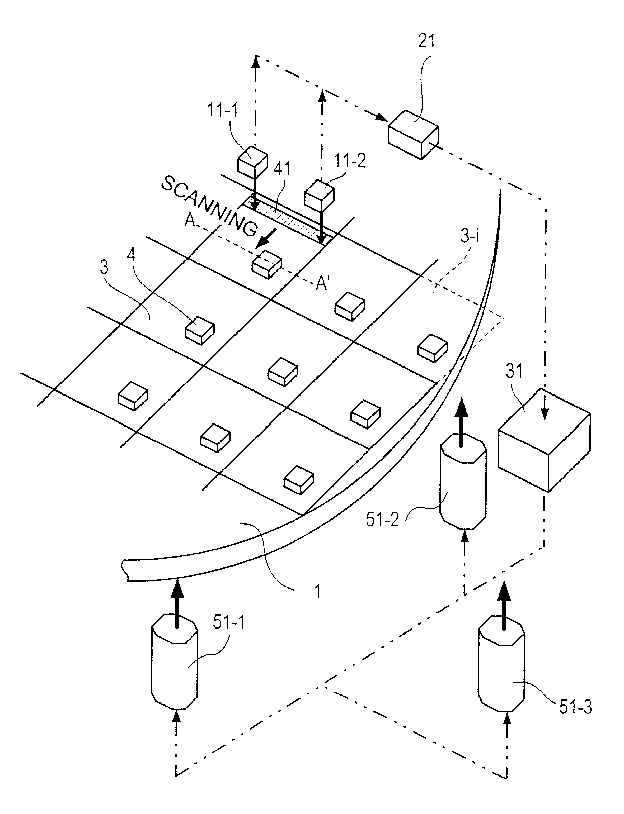
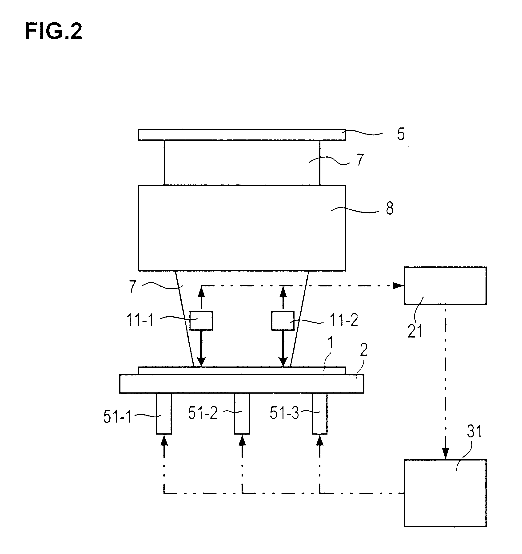
The stepper and the exposure method achieved in the first embodiment of the present invention are explained. It is to be noted that the stepper in the embodiment assumes a structure equivalent to that of the stepper shown in FIGS. 1.about.3 except for in the components explained below.

FIG. 5 is a flowchart provided to facilitate an explanation of the individual steps implemented in the exposure method in the embodiment. The following is the explanation of the individual steps taken in the exposure method in the embodiment.

First, the wafer 1 is loaded at the stepper (step S10) and the loaded wafer 1 is then aligned (step S30).

Next, one shot (measurement target unit area) 3-k is selected from the shots 3-1.about.3-n (step S50). At this time, incomplete shots including the shot 3-i are excluded from the selection.

One sensor head, e.g., the sensor head 11-1, is selected from the four sensor heads 11-1, 11-2, 12-1 and 12-2 secured to the exposure slit 9. Utilizing the s...

second embodiment

(Second Embodiment)

Next, the stepper and the exposure method achieved in the second embodiment of the present invention are explained.

The stepper in the second embodiment is provided with a greater number of photosensor heads compared to the stepper achieved in the first embodiment. More specifically, it includes m sensor heads 11-1.about.11-m which are engaged in operation when the scanning operation is performed along direction A and m sensor heads 12-1.about.12-m which are engaged in operation when the scanning operation is performed along direction B, all provided at the exposure slit 9. It is to be noted that the sensor head 11-1 and the sensor head 12-1 are set on a single line extending along the scanning direction, and that the remaining sensor heads a 11-2.about.11-m and sensor heads 12-2.about.12-m respectively achieve the same positional relationship.

FIG. 7 is a flowchart provided to facilitate an explanation of the individual steps implemented in the exposure method in t...

third embodiment

(Third Embodiment)

The stepper and the exposure method achieved in the third embodiment of the present invention are now explained.

As in the stepper in the first embodiment, four sensor heads 11-1, 11-2, 12-1 and 12-2 are provided at the exposure slit 9 in the stepper in the third embodiment. However, as illustrated in FIG. 8, the sensor heads 11-1, 11-2, 12-1 and 12-2 are each capable of moving along a direction perpendicular to the scanning direction.

FIG. 9 is a flowchart provided to facilitate an explanation of the individual steps implemented in the exposure method in the embodiment. The following is the explanation of the individual steps taken in the exposure method in the embodiment.

First, the wafer 1 is loaded at the stepper (step S10) and the loaded wafer 1 is then aligned (step S30).

Next, one shot 3-k is selected from the shots 3-1.about.3-n (step S50). At this time, incomplete shots including the shot 3-i are excluded from the selection.

One sensor head, e.g., the sensor he...


PUM

PropertyMeasurementUnit
areasaaaaaaaaaa
areaaaaaaaaaaa
distanceaaaaaaaaaa

Abstract

An exposure apparatus and an exposure method that minimize the range over which exposing light becomes defocused even when a non-level portion is present within each shot are provided. One shot is selected from a plurality of shots (exposure unit areas) set on a wafer (S 50). 49 measurement points are set in the selected shot and the three-dimensional coordinates of each measurement point are determined (S 70). Next, an arithmetic operation is performed using the 49 sets of three-dimensional coordinate data to ascertain an "in-shot focus plane" (S 90). This arithmetic operation may be performed through, for instance, the method of least squares. The extents of positional deviation between the surface of the selected shot and the in-shot focus plane is ascertained and the extents of deviation are stored in memory as "adjustment values" (S 110). An exposure shot to undergo exposure processing is selected and the surface level variation manifesting at the exposure shot is measured. The adjustment values are subtracted from the results of the measurement and exposing light is irradiated on the exposure shot while moving the wafer along the vertical direction in conformance to the result of the subtraction (S 130).

Description

1. Field of the InventionThe present invention relates to an exposure apparatus and an exposure method.2. Description of the Related ArtDuring a photolithography process, which is one of the manufacturing processes implemented to manufacture semiconductor devices, a reduction projection exposure apparatus (stepper) is utilized. In keeping with the miniaturization of semiconductor devices achieved in recent years, rigorous efforts are made to reduce the wavelength of the exposing light and to achieve a higher NA (numerical aperture) in the stepper.The relationship between the resolving power R of the stepper and the depth of focus (DOF) is expressed through a Rayleigh formulae presented below.R=k.sub.1 *.lambda. / NADOF=k.sub.2 *.lambda. / (NA).sup.2As these formulae clearly indicate, the focal depth DOF becomes reduced if the wavelength .lambda. of the exposing light is reduced or the numerical aperture NA is increased to improve the resolving power R. Since the focal depth DOF of the s...

Claims


Application Information

Patent Timeline
Patent Type & Authority Patents(United States)
IPC IPC(8): G03B27/42G03F7/20G01B21/00G03F7/207G03F7/22G03F9/02H01L21/027
CPCG03B27/42G03F7/70483
Inventor MORIYAMA, NORIO
Owner LAPIS SEMICON CO LTD
Why Eureka
Try Eureka