Chemical mechanical polishing with electrochemical control

a technology of mechanical polishing and electrochemical control, which is applied in the direction of electrochemical machining apparatus, metal-working apparatus, metallic material coating process, etc., can solve the problems of static etching of the surface of the wafer exposed to the slurry, increase the overall cost of the cmp process, and the conventional cmp process sometimes does not proceed according to specified time periods

Inactive Publication Date: 2004-04-20
ADVANCED MICRO DEVICES INC
View PDF19 Cites 65 Cited by
  • Summary
  • Abstract
  • Description
  • Claims
  • Application Information

AI Technical Summary

Problems solved by technology

The need for frequent replenishment, of course, increases the overall cost of the CMP process and can lead to variations in the slurry composition used for, and therefore the polish rates of, successive wafers in a given lot or for successive lots.
However, conventional CMP processes sometimes do not proceed according to specified time periods.
Process aborts are a leading cause of such variations.
However, during an abort, the chemical activity associated with the CMP slurry may continue, resulting in a static etch of the surfaces of the wafer exposed to the slurry.
This can result in unwanted and substantial etch attack of various structures on the wafer.
Another drawback associated with the conventional slurries is the need for the inclu

Method used


Image

  • Chemical mechanical polishing with electrochemical control
  • Chemical mechanical polishing with electrochemical control
  • Chemical mechanical polishing with electrochemical control

Examples


Embodiment Construction

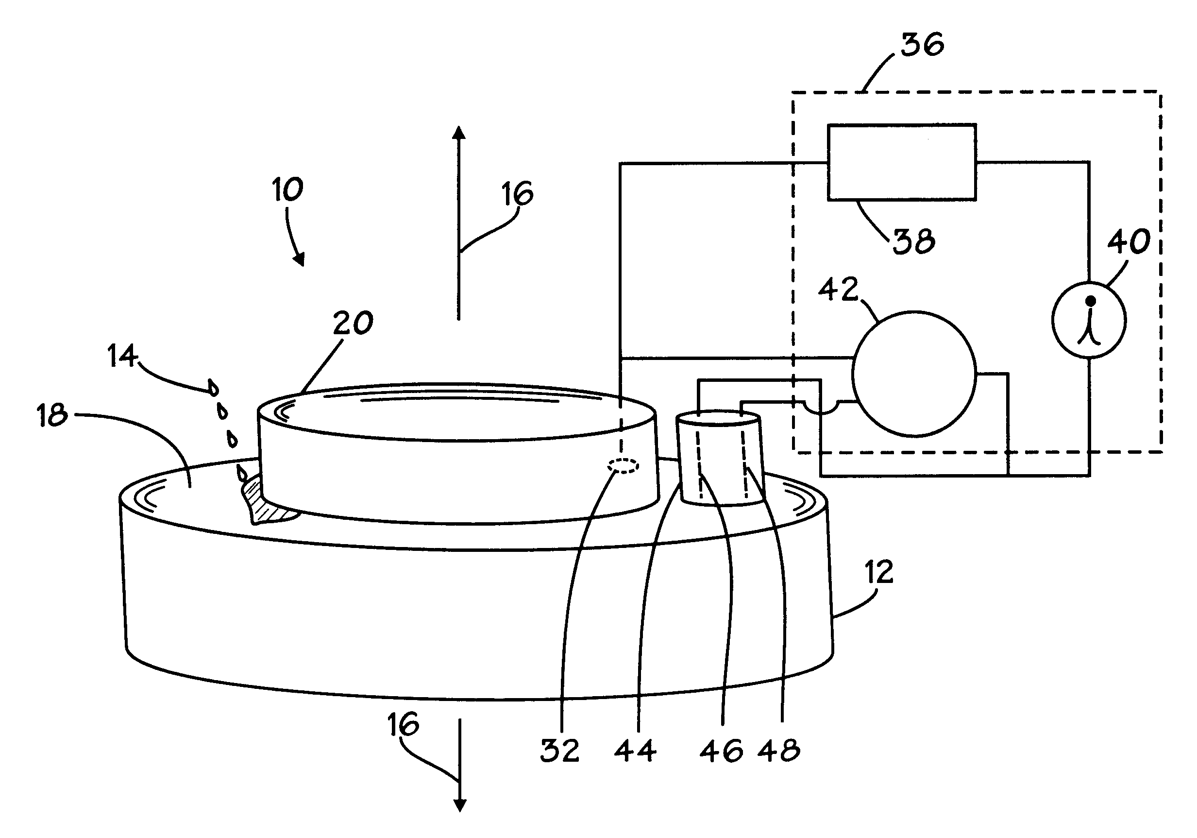
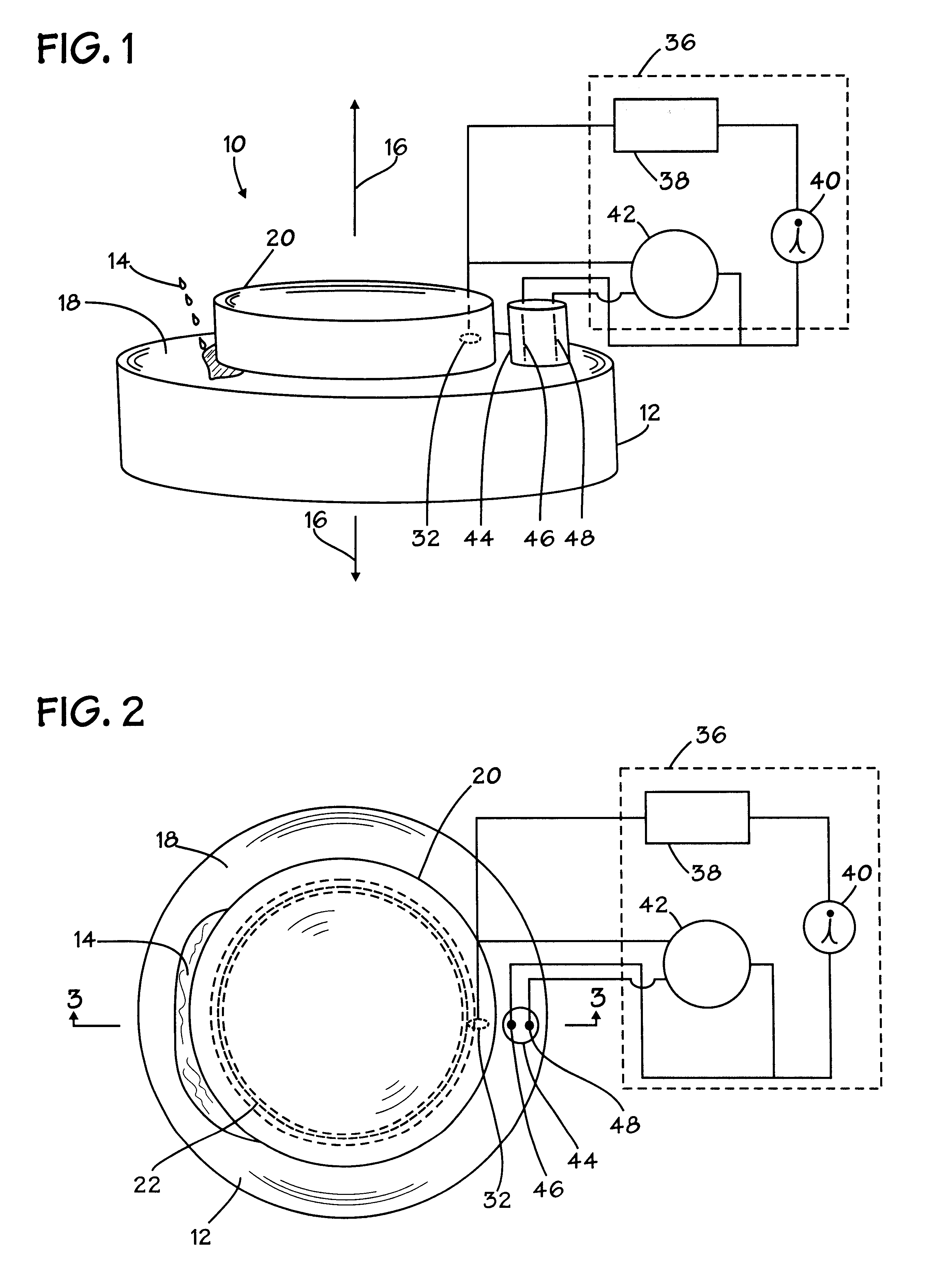
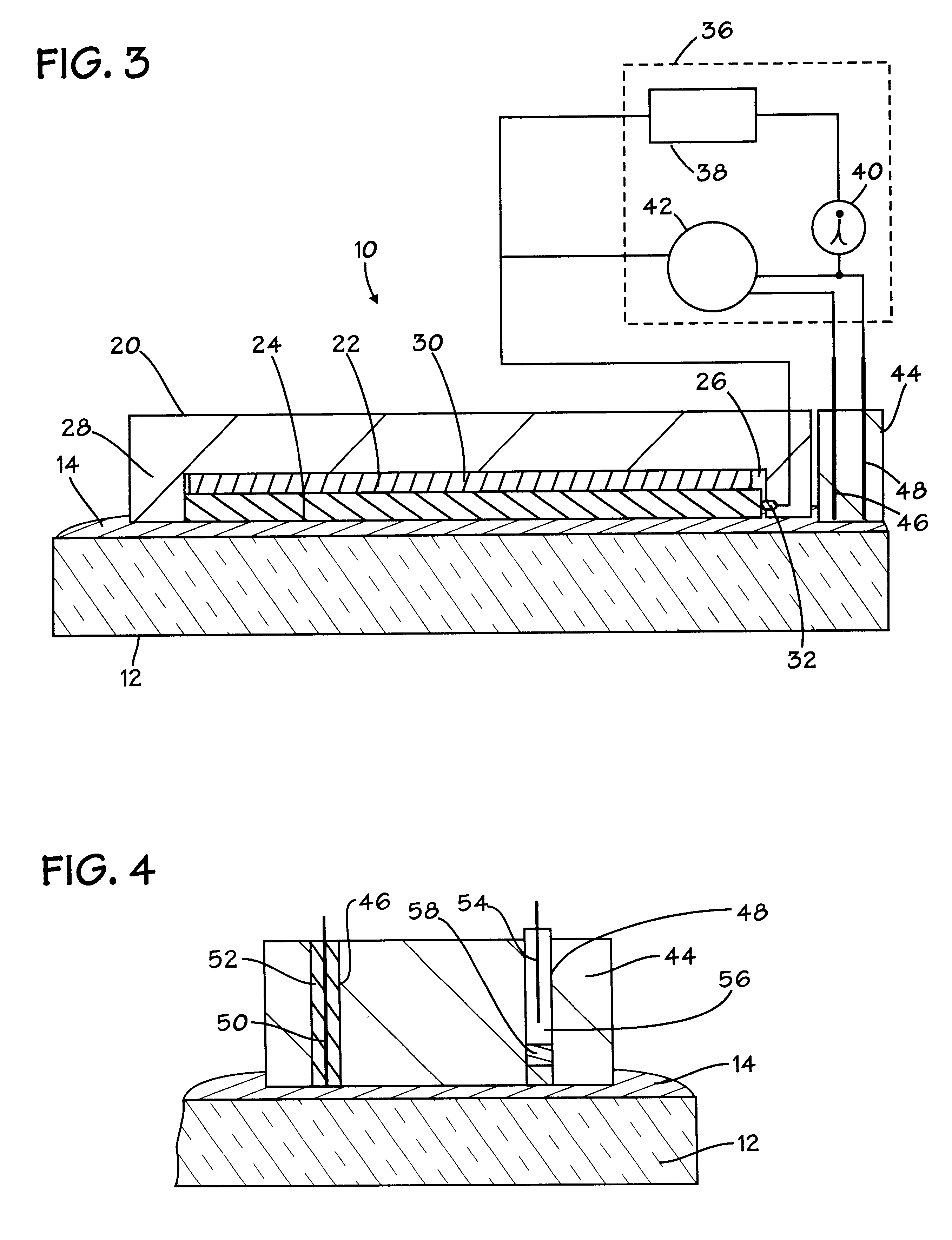
In the drawings described below, reference numerals are generally repeated where identical elements appear in more than one figure. FIG. 1 is a pictorial view of an exemplary embodiment of a chemical mechanical polishing system 10 (hereinafter CMP system 10) that utilizes electrochemistry for the oxidation aspects of CMP in accordance with the present invention. For better understanding, FIG. 1 should be viewed in conjunction with FIG. 2, which is an overhead view of the CMP system 10, and with FIG. 3, which is a cross-sectional view of FIG. 2 taken at section 3--3. The CMP system 10 includes a table 12 that is operable to receive a quantity of a electrically conducting solution 14 dispensed from a reservoir or other dispensing system (not shown). The table 12 may be motorized and therefore operable to rotate about an axis 16. An upper surface 18 of the table 12 functions as a polish pad surface and will typically be composed of a compliant material such as, for example, rubber, syn...


PUM

PropertyMeasurementUnit
Electrical conductoraaaaaaaaaa
Electric potential / voltageaaaaaaaaaa
Abrasiveaaaaaaaaaa

Abstract

Various embodiments of a planarization device and methods of using the same are provided. In one aspect, a device for planarizing a surface of a semiconductor workpiece is provided that includes a table for holding a quantity of an electrically conducting solution thereon. A member is included for holding the semiconductor workpiece such that the surface is in contact with the solution and operates as a working electrode. The member has a first conductor for establishing electrical connection with the semiconductor workpiece. A counter electrode is provided for making electrical connection with the solution and a reference electrode is provided for making electrical connection with the solution with a known electrode potential. A power source is operable to control the electric potential between the working electrode and the counter electrode. Slurry consumption may be dramatically reduced and static etch rate due to aborts may be virtually eliminated.

Description

1. Field of the InventionThis invention relates generally to semiconductor processing, and more particularly to a chemical mechanical polishing system utilizing electrochemistry and to methods of using the same.2. Description of the Related ArtConventional chemical mechanical polishing ("CMP") is, as the name implies, an amalgam of chemical and mechanical processes used to planarize wafer surfaces in semiconductor fabrication. In most conventional CMP processes, a quantity of slurry is deposited on a table or platen of a CMP machine or "polisher." The table has a polish pad that is composed of a compliant or semi-compliant material that partially conforms to the varied topography of a wafer film. Thereafter, the semiconductor wafer is brought into contact with the slurry and the polish pad and relative motion is provided between the wafer and the polish pad.Conventional slurries normally contain several components, such as one or more types of abrasive particles, a stabilizer that i...

Claims


Application Information

Patent Timeline
IPC IPC(8): B24B37/04H01L21/02H01L21/70H01L21/768H01L21/321B23H5/08
CPCB23H5/08B24B37/046H01L21/32125H01L21/7684
Inventor LANSFORD, CHRISTOPHER H.LANSFORD, JEREMY S.YELLITZ, BRADLEY J.
Owner ADVANCED MICRO DEVICES INC
Why Eureka
Try Eureka