

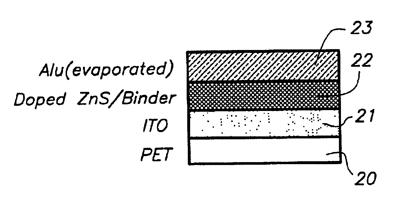
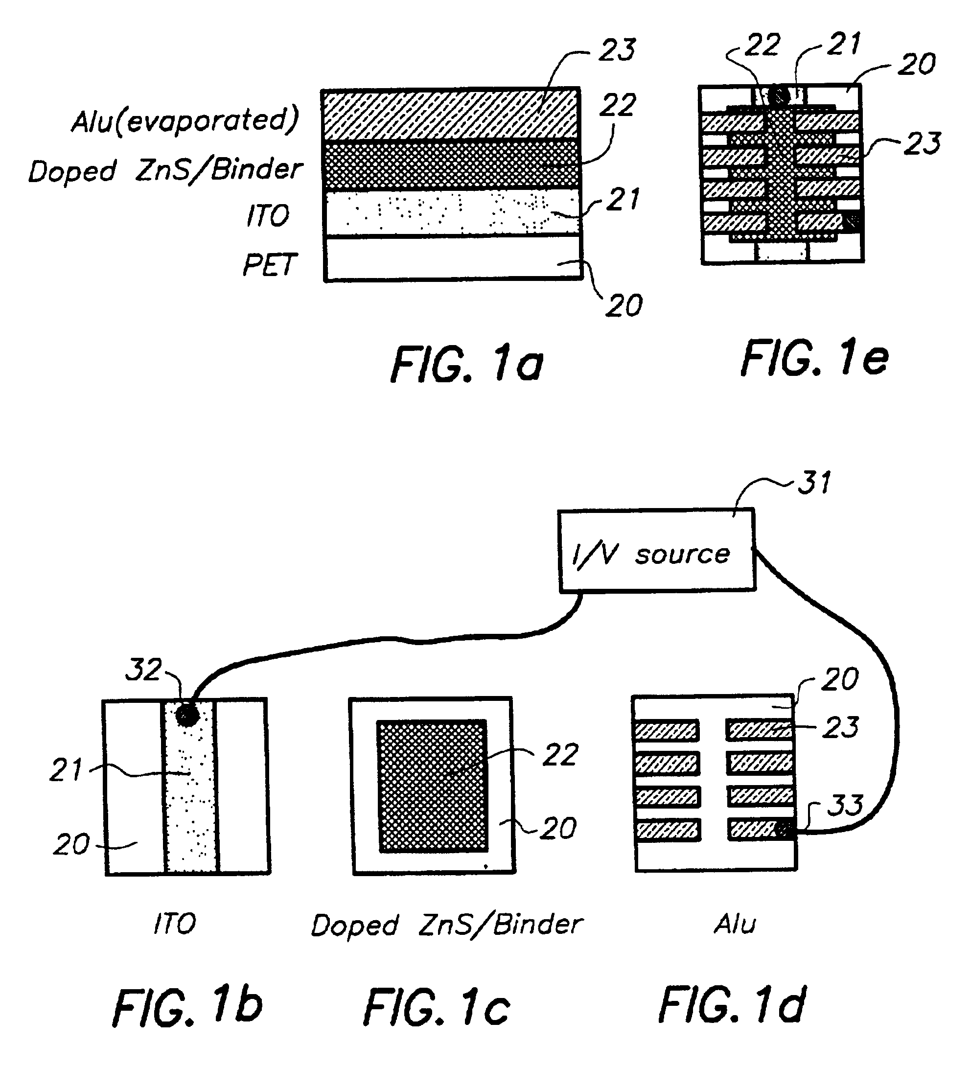
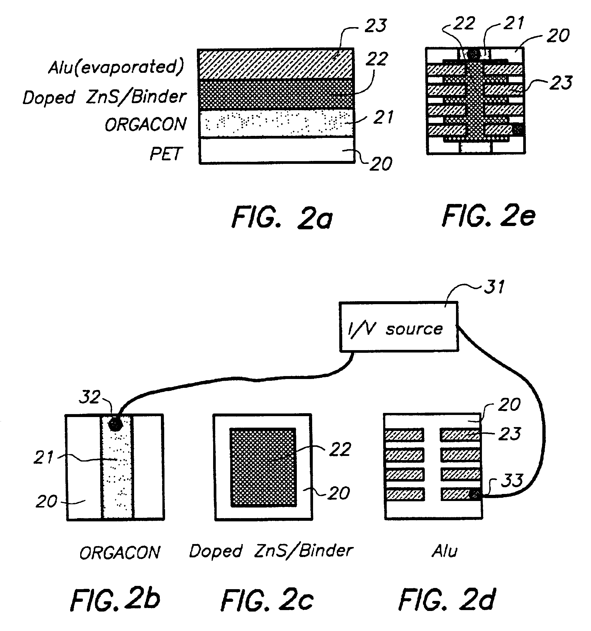
Manufacturing of a thin film inorganic light emitting diode
a technology of inorganic light and diodes, which is applied in the manufacture of electric discharge tubes/lamps, hose connections, and discharge tubes luminescnet screens, etc., can solve the problems of low fluorescent quantum yield, cumbersome and expensive vacuum-vapour deposition techniques, and low fluorescent quantum yield of tfel devices, etc., to achieve easy and economical
- Summary
- Abstract
- Description
- Claims
- Application Information
AI Technical Summary
Benefits of technology
Problems solved by technology
Method used
Image

Examples
Embodiment Construction
1. Green emitting single layer ILEDs
1.1. Preparation of the Zn(Cu(0.05%))S-Dispersion:
The following solutions were prepared:
The ZnS:Cu(0.05%) dispersion was prepared as follows:
To solution 3, stirred at 1500 rpm at room temperature solutions 1 and 2, both held at room temperature, were added simultaneously at a flow rate of 500 ml / min. This is the predispersion A comprising ZnS:Cu--particles.
1.2. Washing of the ZnS:Cu--Dispersion:
To 1000 ml of predispersion A, 1000 ml of a 2% polyphosphoric acid solution in water was added and this dispersion was diafiltrated through a Fresenius F60 cartridge. The dispersion was concentrated to 1000 ml and washed at this level by using 5000 ml of a 2% solution of polyphosphoric acid in water.
After the washing, this dispersion was concentrated by means of the diafiltration set-up to a concentration of about 40 g ZnS / l. Subsequently, 1 ml of a 12.5% solution of Saponine Quillaya (Schmittmann) in water / ethanol (80 / 20) solution of per 20 ml dispersion w...
PUM
| Property | Measurement | Unit |
|---|---|---|
| thick | aaaaa | aaaaa |
| thick | aaaaa | aaaaa |
| thick | aaaaa | aaaaa |
Abstract
Description
Claims
Application Information