Ultra thin back-illuminated photodiode array structures and fabrication methods
- Summary
- Abstract
- Description
- Claims
- Application Information
AI Technical Summary
Benefits of technology
Problems solved by technology
Method used
Image

Examples
Embodiment Construction
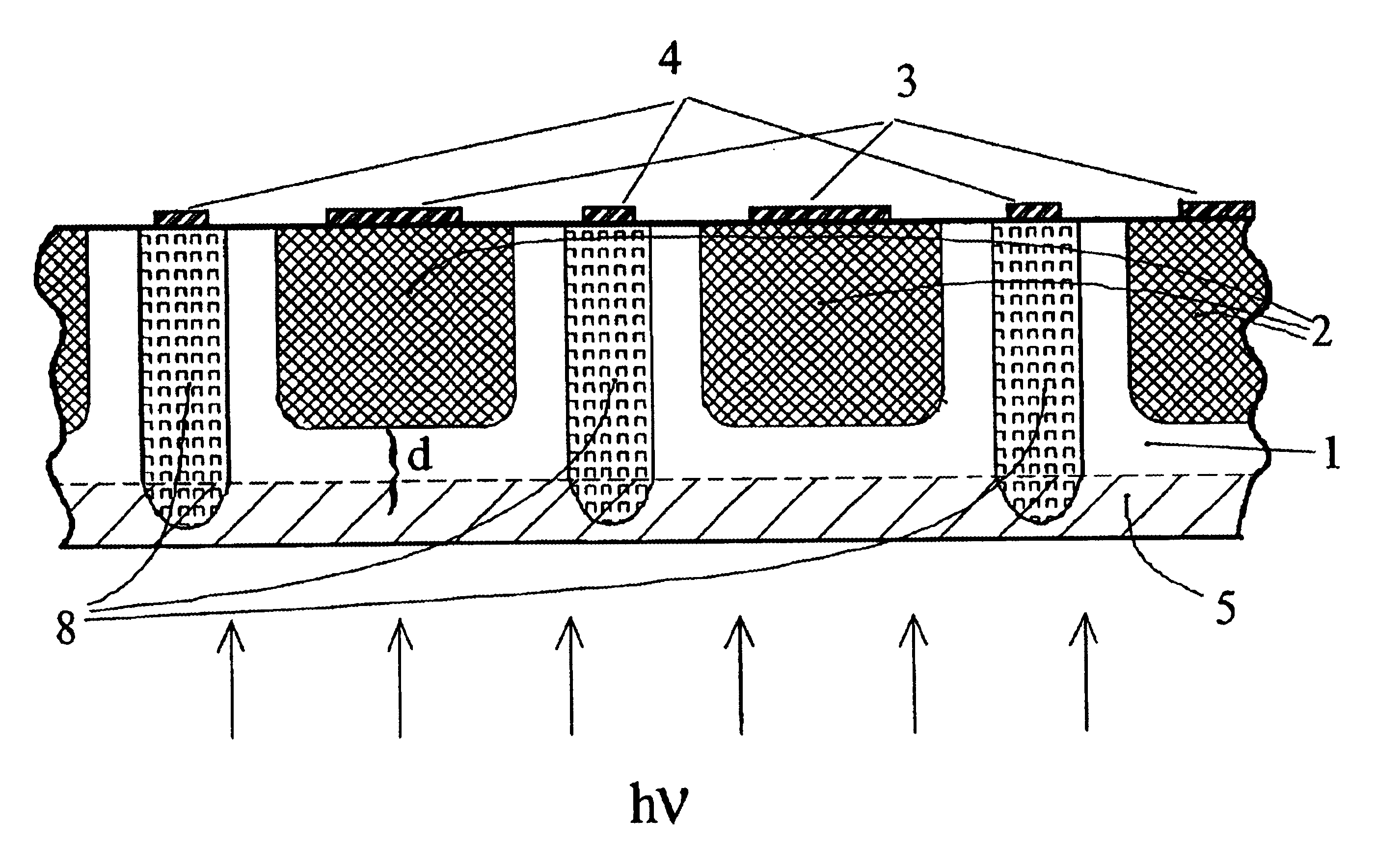
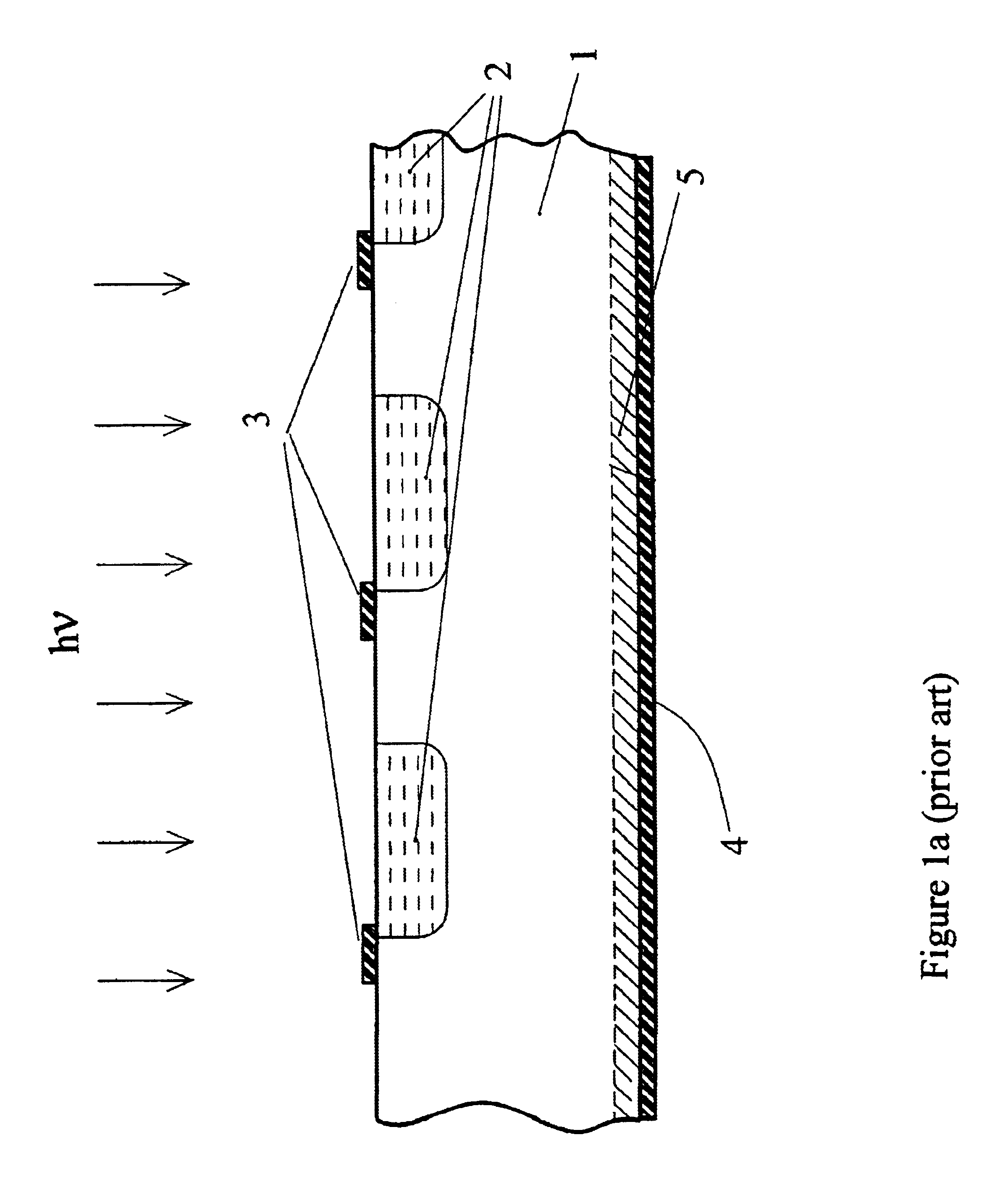
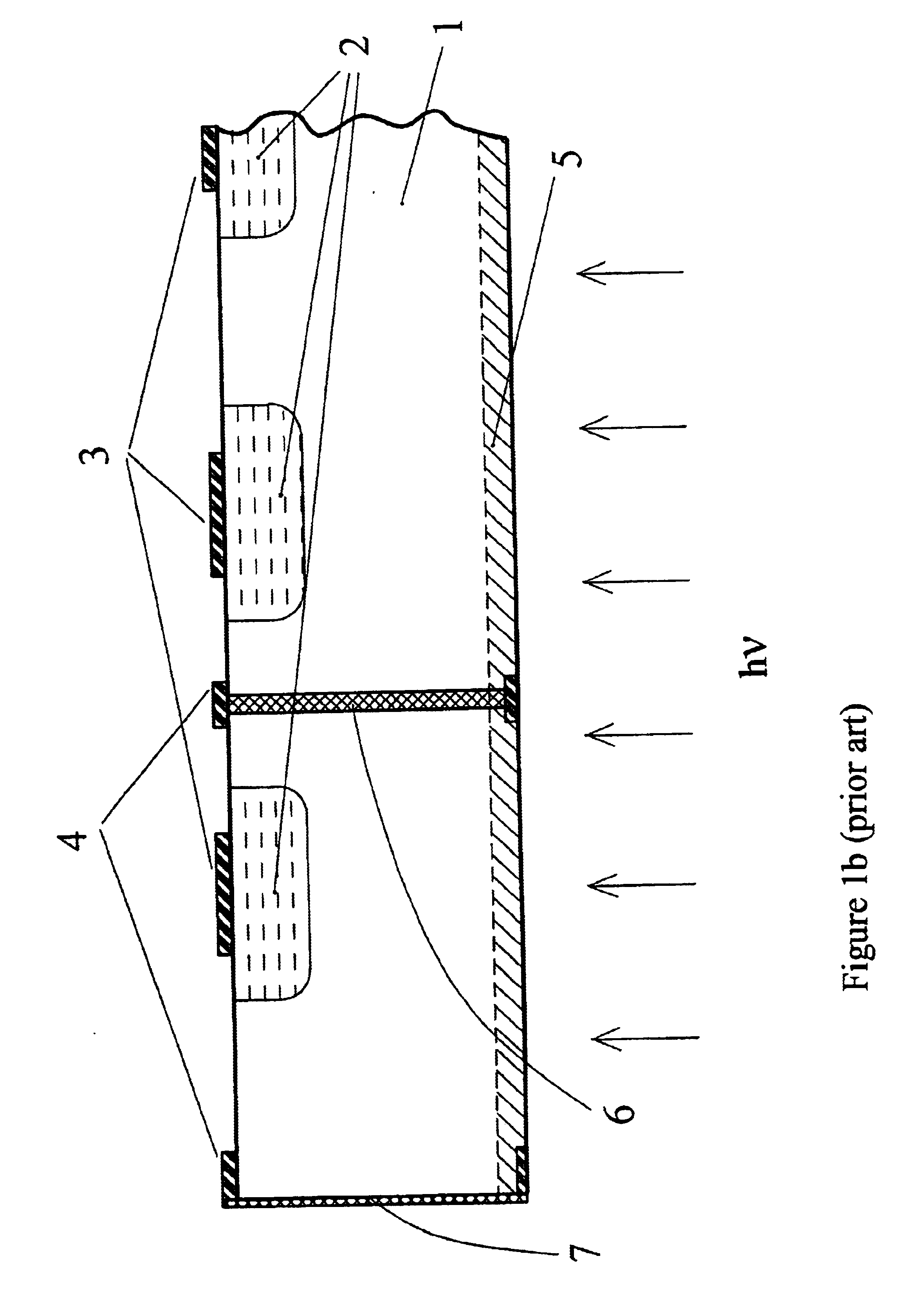
FIG. 2 is a simplified cross-sectional view of a semiconductor ultra-thin chip photodiode array in accordance with a preferred embodiment of the present invention. The structure is built using either n-type or p-type bulk silicon 1. For brevity, the anode in the case of p-on-n structure or the cathode in the case of n-on-p structure will be referred to as "the first electrode", while the cathode in the case of p-on-n structure and the anode in the case of n-on-p structure will be referred to as "the second electrode."
The material resistivity, thickness of the wafer / die, dopants concentrations and doses, and diffusion conditions are preferably chosen to satisfy the following requirements:
a) The active area (the first electrode) diffusion 2 extends sufficiently close to the back surface of the finished die that the rest of the volume between the diffusion edge and the blanket implant in the die back surface and part of the blanket implant, the space indicated as "d" in the FIG. 2, bec...
PUM
 Abstract
Description
Claims
Application Information
 - R&D Engineer
- R&D Manager
- IP Professional
- Industry Leading Data Capabilities
- Powerful AI technology
- Patent DNA Extraction
Browse by: Latest US Patents, China's latest patents, Technical Efficacy Thesaurus, Application Domain, Technology Topic.
© 2024 PatSnap. All rights reserved.Legal|Privacy policy|Modern Slavery Act Transparency Statement|Sitemap