Methods of writing/erasing of nonvolatile semiconductor storage device

Inactive Publication Date: 2004-07-27
RENESAS ELECTRONICS CORP
View PDF6 Cites 7 Cited by
  • Summary
  • Abstract
  • Description
  • Claims
  • Application Information

AI Technical Summary

Problems solved by technology

(1) To set the memory transistor MT(n) to a high threshold voltage Vthp in writing, the N.sup.+ diffusion region 105(n) is set at 5 V, the N.sup.+ diffusion region 105(n+1) at 0 V, the access gate 107a(n) at 2 V, and the access gates 107a(n-1) and 107a(n+1) at 0 V.

Method used


Image

  • Methods of writing/erasing of nonvolatile semiconductor storage device
  • Methods of writing/erasing of nonvolatile semiconductor storage device
  • Methods of writing/erasing of nonvolatile semiconductor storage device

Examples


Embodiment Construction

>

(Configuration)

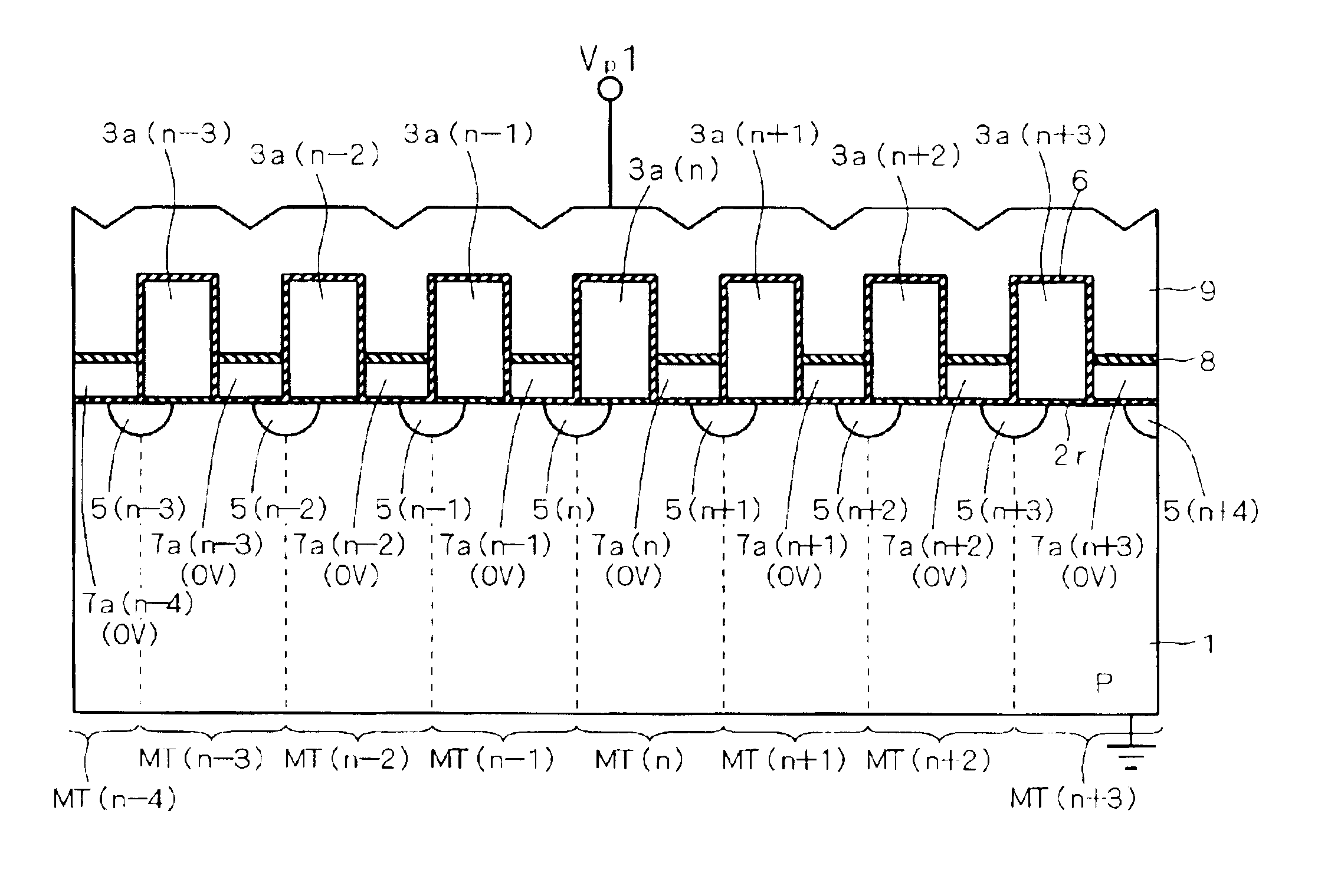
FIG. 1 is a cross-sectional view illustrating a configuration of a group of memory transistors in a flash memory according to one preferred embodiment of the present invention. As shown, a plurality of N.sup.+ diffusion regions 5 (5(n-3) to 5(n+3)) are selectively formed in the surface of a P-type silicon substrate 1. On the surface of the P-type silicon substrate 1, a plurality of floating gates 3a (3a(n-3) to 3a(n+3)) are selectively formed with a silicon oxide film 2r sandwiched in between. Further, a plurality of access gates 7a (7a(n-4) to 7a(n+3)) are selectively formed on the surface of the P-type silicon substrate 1, with a three-layer insulating film 6, consisting of a silicon oxide film, a silicon nitride film, and a silicon oxide film, sandwiched in between.

A silicon oxide film 8 is formed on each of the plurality of access gates 7a, and the plurality of floating gates 3a are covered with the three-layer insulating film 6. Further, a control gate 9 is form...


PUM


Abstract

A nonvolatile semiconductor storage device can achieve a shortened write time and a reduced absolute value of an operating voltage at the time of erasing. A P-type silicon substrate (1) is set at a ground level, a control gate (109) is set at a high voltage (Vp1), and a voltage of 0 V is applied to an access gate line connected in common to all access gates (7a) to set all the access gates (7a(n-4) to 7a(n+3)) at 0 V. When the threshold voltage of a memory transistor (MT(n)) is set into a written state, an N<+> diffusion region (5(n)) is set at 0V. This causes tunnel injection of electrons into a floating gate (3a(n)) of the memory transistor (MT(n)) and thereby allows the memory transistor MT(n) to be set to a high threshold voltage (Vthp) without being influenced by the contents of writing to adjacent memory transistors.

Description

1. Field of the InventionThe present invention relates to a nonvolatile semiconductor storage device, and especially to writing / erasing of memory cells in a flash memory.2. Description of the Background ArtOf electrically rewritable nonvolatile semiconductor storage devices, flash memories capable of erasing the entire or a block of data by one operation are well known in the art. Such flash memories are disclosed for example in Japanese Patent Application Laid-open Nos. 2001-28428, 2001-85540, and 2001-85541.FIGS. 6 to 13 are cross-sectional views illustrating a method of manufacturing a group of memory transistors (memory cells) in a conventional flash memory. Referring to the drawings, the manufacturing procedure will be described hereinbelow.Initially, as shown in FIG. 6, a silicon oxide film 102 is grown to a thickness of about 100 angstroms by thermal oxidation on the surface of a P-type silicon substrate 101 having a (001) crystal orientation, and then a phosphorus-doped poly...

Claims


Application Information

Patent Timeline
Patent Type & Authority Patents(United States)
IPC IPC(8): H01L27/115H01L21/70H01L21/8247G11C16/04H01L29/788H01L29/792
CPCG11C16/0433G11C16/0491H01L27/115H01L27/11521H01L27/11524H10B41/35H10B69/00H10B41/30
Inventor KOBAYASHI, KIYOTERU
Owner RENESAS ELECTRONICS CORP
Why Eureka
Try Eureka